
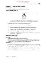


,QVWDOODWLRQ
#
3URFHGXUH
##
60<
953#
9HFWRU
#
'ULYH
#0#
+$
7968;7
&RQWURO
#
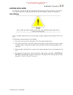
:LULQJ
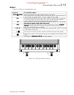
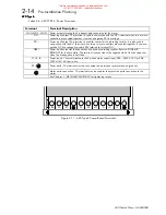
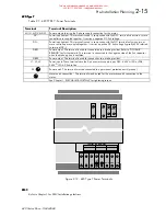
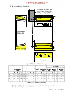
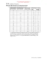
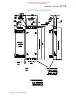
General wiring diagrams for the 620 are provided in Chapter 2.
Control cables should be 0.75mm
2
(18AWG) minimum. It is recommended that screened cable is used, with the
screen connected at the drive end only. Control wiring should be kept separate from power and motor wiring.
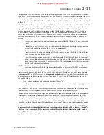
For normal speed control operation, the speed demand signals are connected to the speed inputs (control board
terminals C3, C4 and F2) as required. Terminal C2 or F1 may be used for the 0V connection associated with the
SPEED SETPOINT and DIRECT INPUT signals. The maximum speed, and other associated parameters, are set
from the MMI.
The START signal to the 620 Vector drive is provided by connecting a single holding contact between control board
terminal B7 (START) and terminal B9 (+24V). When the contact is open, the motor stops. When the contact is
closed and both COAST STOP and FAST STOP are at +24V, the motor will run.
A digital output indicating that the drive is healthy is provided on terminals E7 of the 620 Vector drive. Any alarm
which causes the drive healthy output to de-activate is internally latched by the drive until both START and JOG go
low (0V or open circuit). The cause of the alarm is displayed by the MMI. Once latched, such an alarm can be
cleared only by removing and re-applying the START or JOG signal.
'<1$0,&
#
%5$.,1*
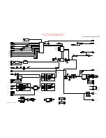
,QWURGXFWLRQ
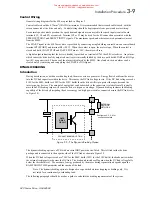
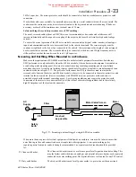
During deceleration, or with an overhauling load, the motor acts as a generator. Energy flows back from the motor
into the DC link capacitors within the drive. This causes the DC link voltage to rise. If the DC link voltage exceeds
810V for the 400V build (or 420V for the 230V build) then the drive will trip to protect the capacitors and the
inverter power devices. The amount of energy that can be absorbed in the capacitors is relatively small; typically
more than 20% braking torque will cause the drive to trip on overvoltage. Dynamic braking increases the braking
capability of the drive by dissipating the excess energy in a high power resistor connected across the DC link (refer
to Figure 3.2).
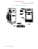
DYNAMIC BRAKING OPTION
GATE
DRIVE
CIRCUIT
+
EXTERNAL
RESISTOR
NETWORK
See figures 2.3 - 2.6 for
connection details
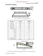
)LJXUH
#615#0#
7KH
#
'\QDPLF
#
%UDNLQJ
#
2SWLRQ
The dynamic braking option is a PCB with an extra IGBT power device fitted. This is fitted inside the drive
package and is connected to the negative side of the DC link as shown in Figure 3.2.
When the DC link voltage rises above 750V for the 400V build (385V for the 230V build), the brake unit switches
the external resistor network across the DC link. The brake unit switches off again when the DC link voltage falls
below the threshold level. The amount of energy produced by the motor during regeneration depends upon the
RAMP DOWN TIME parameter and the inertia of the load.
Note: The dynamic braking option is designed to cope with short term stopping or braking only. It is
not rated for a continuously overhauling load.
The following paragraphs should be used as a guide to calculate the braking requirements of the system.
This manual was downloaded on www.sdsdrives.com
+44 (0)117 938 1800 - [email protected]