


7/30/2019
Cora Z7 Reference Manual [Reference.Digilentinc]
https://reference.digilentinc.com/reference/programmable-logic/cora-z7/reference-manual?_ga=2.21685883.1349070004.1564406803-1961480359.… 20/23
Absolute
Minimum Voltage
Recommended Minimum
Operating Voltage
Recommended Maximum
Operating Voltage
Absolute
Maximum Voltage
Powered
-0.4 V
-0.2 V
3.4 V
3.75 V
Unpowered
-0.4 V
N/A
N/A
0.55 V
Table 13.1.1. Shield Voltage Specifications
(https://www.xilinx.com/support/documentation/data_sheets/ds190-Zynq-7000-Overview.pdf)
The pins on the shield connector typically used for I2C signals are labeled as SCL and SDA. On the Cora Z7, these signals are each attached
to a pull-up resistor. While these pins can still be used as digital I/O, these pull-ups should be kept in mind.
The pins labeled A0-A11 and V_P/V_N are used as analog inputs to the XADC module of the FPGA. The FPGA expects that the inputs
range from 0-1 V. On the pins labeled A0-A5, the Cora Z7 uses an external circuit to scale down the input voltage from 3.3V. This circuit is
shown in Figure 13.2.1. This circuit allows the XADC module to accurately measure any voltage between 0V and 3.3V (relative to the Cora
Z7's GND ()) that is applied to any of these pins. The pins labeled A0-A5 can also be used as digital inputs or outputs, as they are also
connected directly to the FPGA before the resistor divider circuit (also shown in Figure 13.2.1).
Figure 13.2.1. Single-Ended Analog
Inputs
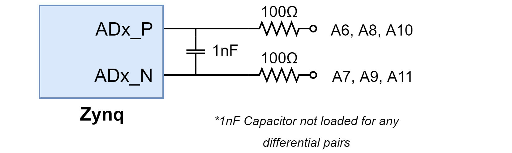
The pins labeled A6-A11 are connected directly to 3 pairs of analog capable pins on the FPGA via an anti-aliasing filter. This circuit is
shown in Figure 13.2.2. These pairs of pins can be used as differential analog inputs with a voltage difference between 0-1V. The even-
numbered pins are connected to the positive pins of the trio and the odd numbers are connected to the negative pins (so A6 and A7 form
an analog input pair with A6 being positive and A7 being negative). Note that though the pads for the capacitor are present, they are not
loaded for these pins. Since the analog capable pins of the FPGA can also be used like normal digital FPGA pins, it is also possible to use
these pins for Digital I/O.
Figure 13.2.2. Differential Analog Inputs
The pins labeled V_P and V_N are connected to the VP_0 and VN_0 dedicated analog inputs of the FPGA. This pair of pins can also be
used as a differential analog input with voltage between 0-1V, but they cannot be used as Digital I/O. The capacitor in the circuit shown in
Figure 13.2.3 for this pair of pins is loaded on the Cora Z7.
13.2 Shield Analog I/O