EE PRO for TI-89, 92 Plus
Equations - Solid State Devices
84
66
A-
8C
A8
%QORWVGF4GUWNVU
%L
'A(
8DK
A8
ZF
'AO
ZP
'AO
ZR
'AO
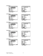
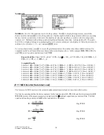
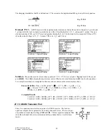
Example 27.2.2 -
A linearly graded junction has an area of 100
µ
2
, a built-in voltage of 0.8578 V, and an applied
voltage of -5.V. The relative permittivity of silicon is 11.8. Under room temperature conditions, what is the junction
capacitance, depletion layer width, and the linear-graded junction parameter?
Entered Values
Calculated Results
Solution -
Use equations 27.2.5-7 to compute the solution for this problem. Select these by highlighting each
equation and pressing the
¸
key. Press
„
to display the input screen, enter all the known variables and press
„
to solve the equations. The computed results are shown in the screen displays above.
-PQYP8CTKCDNGU8C
A8
8DK
A8
#L
A
µ
@
εε
U
66
A
°
-
%QORWVGF4GUWNVU
C.),
'AO@
%L
'A(
ZF
A
µ
27.3 PN Junction Currents
These equations characterize the relationships for computing currents in PN junctions. They can be classified into four
categories.
The first three equations define the junction currents. First, the junction current I is expressed in terms of the junction
area Aj, diffusion coefficients Dn and Dp, diffusion lengths LLn and Lp, equilibrium densities of minority carriers
npo and pno, applied bias Va, and temperature TT. The second equation is a simplified form the first equation where
the current I0 is defined as the multiplier of the exponential term. In this form, it is often called Shockley equation.
The third equation calculates this saturation current I0 in terms of the junction area Aj, diffusion coefficients Dn and
Dp, diffusion lengths LLn and Lp, equilibrium densities of minority carriers npo and pno. It is used to simplify the
first equation.
I
q Aj
Dn
LLn
npo
Dp
Lp
pno
e
q Va
k TT
= ⋅ ⋅
⋅
+
⋅
F
HG
I
KJ
⋅
−
F
HG
I
KJ
⋅
⋅
1
Eq. 27.3.1
I
I
e
q Va
k TT
=
⋅
−
F
HG
I
KJ
⋅
⋅
0
1
Eq. 27.3.2
I
q Aj
Dn
LLn
npo
Dp
Lp
pno
0
= ⋅ ⋅
⋅
+
⋅
F
HG
I
KJ
Eq. 27.3.3


