background image

20

DS1113F1

CS4399

3 Characteristics and Specifications

Rise time of SCL and SDA

Standard Mode

Fast Mode

Fast Mode Plus

t

RC


1000

300
120

ns
ns
ns

Fall time of SCL and SDA

Standard Mode

Fast Mode

Fast Mode Plus

t

FC


300
300
120

ns
ns
ns

Setup time for stop condition

t

SUSP

260

ns

SDA setup time to SCL rising

t

SUD

50

ns

SDA input hold time from SCL falling 

4

t

HDDI

0

ns

Output data valid (Data/Ack) 

5

Standard Mode

Fast Mode

Fast Mode Plus

t

VDDO


3450

900
450

ns
ns
ns

Bus free time between transmissions

t

BUF

500

ns

SDA bus capacitance

SCL frequency = 1 MHz, V

L

 = 1.8 V

SCL frequency 

 400 kHz

C

B


400
400

pF
pF

SCL/SDA pull-up resistance 

1

V

L

 = 1.8 V

R

P

350

Pulse width of spikes to be suppressed 

t

PS

50

ns

Switching time between RCO and MCLK_INT 

6

150

µs

Power-up delay (delay before I

2

C can communicate after RESET released)

t

PUD

1500

µs

1.The minimum R

P

 value (resistor shown in 

Fig. 2-1

) is determined by using the maximum level of VL, the minimum sink current strength of its 

respective output, and the maximum low-level output voltage V

OL

. The maximum R

P

 value may be determined by how fast its associated signal must 

transition (e.g., the lower the value of R

P

, the faster the I

2

C bus is able to operate for a given bus load capacitance). See I²C bus specification 

referenced in 

Section 13

.

2.All timing is relative to thresholds specified in 

Table 3-8

, V

IL

 and V

IH

 for input signals, and V

OL

 and V

OH

 for output signals.

3.I²C control-port timing

4.Data must be held long enough to bridge the transition time, t

F

, of SCL.

5.Time from falling edge of SCL until data output is valid.

6.Upon setting MCLK_SRC_SEL and sending the I

2

C stop condition, the switching of RCO and other MCLK_INT sources occurs. A least wait 

time as specified is required after changing MCLK_SRC_SEL and sending the I

2

C stop condition before the next I

2

C transaction is initiated. 

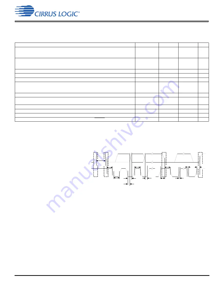
Table 3-17. I

2

C Slave Port Characteristics

 (Cont.)

Test conditions (unless specified otherwise): 

Fig. 2-1

 shows typical connections; Inputs: GNDA = GNDL = GNDCP = 0 V; all voltages with respect to 

ground; VL = 1.8 V; inputs: Logic 0 = GNDA = 0 V, Logic 1 = VL; T

A

 = +25°C; SDA load capacitance equal to maximum value of C

B

= 400 pF; minimum 

SDA pull-up resistance, R

P(min)

.

1


Table 3-1

 describes some parameters in detail. All specifications are valid for the signals at the pins of the CS4399 with 

the specified load capacitance. 

Parameter 

2

Symbol 

3

Minimum

Maximum

Units

t

BUF

t

LOW

Stop

t

HDDI

t

SUD

t

SUST

t

RC

t

HDST

t

HIGH

t

HDST

t

FC

t

SUSP

Start

Repeated 

Start

Stop

SDA

SCL

t

VDDO

Summary of Contents for CS4399

Page 1: ...Low latency mode minimizes pre echo 110 dB of stopband attenuation Supports sample rates from 32 to 384 kHz I2S right justified left justified TDM and DSD over PCM DoP interface Master or slave operation Volume control with 0 5 dB step size and soft ramp 44 1 kHz deemphasis and inverting feature 40 pin QFN or 42 ball CSP package option Applications Smart phones tablets portable media players lapto...

Page 2: ...audio integrity by allowing signal processing such as volume control and 50 kHz Scarlet Book recommended filtering to be applied directly to the DSD stream without an intermediate decimation stage Additional features like volume matching and channel mixing enable seamless transition between DSD and PCM playback paths The CS4399 accepts I2S right justified left justified and TDM format PCM data at ...

Page 3: ...eristics 19 4 Functional Description 21 4 1 Overview 21 4 2 Analog Outputs 23 4 3 Class H Output 24 4 4 Headphone Presence Detect 27 4 5 Clocking Architecture 29 4 6 Clock Output and Fractional N PLL 31 4 7 Filtering Options 34 4 8 Audio Serial Port ASP 34 4 9 DSD Interface 42 4 10 DSD and PCM Mixing 44 4 11 Standard Interrupts 44 4 12 Control Port Operation 45 5 Applications 48 5 1 PLL Clocking 4...

Page 4: ...n Through Package View 40 Pin QFN Package 21 26 27 28 29 30 22 23 24 25 7 6 5 4 3 2 1 10 9 8 12 11 13 14 15 16 17 18 19 20 39 40 38 37 36 35 34 33 32 31 DSDB LRCK2 RESET VCP FLYP_VCP FLYC_VCP HP_DETECT VCP_FILT SCL SDIN1 TSO VD FILT FILT VA GNDA VA FLYP_VA DSDA SDIN2 SDA LRCK1 XTI MCLK XTO GNDD SCLK1 CLKOUT DSDCLK SCLK2 REFA AOUTA GNDCP AOUTB REFB VCP_FILT INT VP VL ADR GNDCP FLYN_VCP FLYN_VA GNDC...

Page 5: ...SDIN1 DSDCLK SCLK2 CLKOUT LRCK1 SDA SCL TSO DSDB LRCK2 ADR GNDD RESET INT VD VP VCP TSI FILT FILT VA FLYP_VCP VCP_FILT REFB REFA GNDA VA FLYC_VCP GNDCP GNDCP HP_DETECT TSI FLYP_VA FLYN_VCP VCP_FILT AOUTB AOUTA GNDCP FLYN_VA A1 A2 A3 A4 A5 A6 B1 B2 B3 B4 B5 B6 C1 C2 C3 C4 C5 C6 D1 D2 D3 D4 D5 D6 E1 E2 E3 E4 E5 E6 F1 F2 F3 F4 F5 F6 G1 G2 G3 G4 G5 G6 Charge Pump Analog I O Digital I O Ground Power Su...

Page 6: ...pulled up works as system interrupt pin Open drain active low programmable CMOS open drain output RESET 28 C4 VP I System Reset The device enters system reset when enabled Hysteresis on CMOS input SDA 39 B4 VL I O Serial Control Data I O I C In I C Mode SDA is the control I O data line CMOS open drain output Hysteresis on CMOS input SCL 1 B5 VL I Software Clock I C Serial control interface clock u...

Page 7: ...p Output Negative charge pump output for DAC rail It is derived from VA FLYP_VA FLYN_VA 10 11 F6 G6 VA O VA Charge Pump Cap Positive Negative Node Positive negative nodes for the DAC negative charge pump s flying capacitor FLYP_VCP 24 E1 VCP VP 1 O VCP Charge Pump Cap Positive Node Positive node for the analog output negative charge pump s flying capacitor FLYC_VCP 23 F1 VCP VP 1 O VCP Charge Pump...

Page 8: ...SD Topology Table 1 2 shows the individual ESD domains and lists the pins associated with each domain ESD sensitive device The CS4399 is manufactured on a CMOS process Therefore it is generically susceptible to damage from excessive static voltages Proper ESD precautions must be taken while handling and storing this device This device is qualified to current JEDEC ESD standards Table 1 2 ESD Domai...

Page 9: ...CP RESET INT VP VCP_FILT FLYP_VCP FLYC_VCP HP_DETECT VCP_FILT VCP_FILT FLYN_VCP AOUTA AOUTB REFA REFB Table 1 2 ESD Domains Cont ESD Domain Signal Name See in Topology Figures for Pad Topology VA VA GNDA Substrate VP VCP_FILT GNDCP VCP_FILT Substrate VP GNDCP Domain VP VCP_FILT Domain VCP_FILT VCP_FILT Domain ...

Page 10: ...P_VCP CLKOUT Audio Devices XTI MCLK XTO See Clocking Configuration FILT FILT 15 µF Battery 3 0 V 5 25 V 2 2 µF FLYC_VCP VP 1 8 V 2 2 µF 2 2 µF 4 7 µF RESET Applications Processor Micro Controller INT RP_I VL ADR SDA SCL VD 0 1 µF 15 µF Clocking Configuration XTAL External MCLK System Clock XTI MCLK XTO 0 1 µF AOUTA REFA AOUTB REFB HP_DETECT VCP_FILT GNDCP VCP VCP_FILT See VCP_FILT Configuration VC...

Page 11: ...grity The load capacitance effectively moves the band limiting pole of the amp in the output stage Increasing load ca pacitance beyond the recommended value can cause the internal op amp to become unstable Output offset voltage The DC offset voltage present at the amplifier s output when its input signal is in a mute state The offset exists due to CMOS process limitations and is proportional to an...

Page 12: ... VCP 1 8 V VL VD 1 8 V VP 3 6 V TA 25 C measurement bandwidth is 20 Hz 20 kHz ASP_SPRATE 0001 LRCK 44 1 kHz mode PDN_XTAL 0 MCLK_INT 1 and MCLK_SRC_SEL 00 crystal frequency fXTAL 22 5792 MHz Volume 0 dB when testing in DSD processor mode DSD_ZERODB 1 when testing noise related specifications dynamic range THD N idle channel noise no external impedance on REFx PCM and DSD Processor Mode Parameter 2...

Page 13: ...kHz sample rates MCLK_INT is an integer multiple of Fs HPF disabled no DC offset applied group delay does not include serial port delay Parameter Minimum Typical Maximum Units Fast Roll Off FILTER_SLOW_FASTB 0 Single Speed Mode 1 Passband 2 to 0 01 dB corner to 3 dB corner attenuation Fs 2 0 0 8 44 3 0 4535 4 0 49 Fs Fs dB Passband ripple 10 Hz to 0 01 dB corner 5 0 01 0 01 dB Stopband 0 547 Fs St...

Page 14: ...OMB_LOWLATB 1 20 7 Fs s Group delay minimum phase PHCOMB_LOWLATB 0 10 6 Fs s Nonoversampling NOS NOS 1 Single Speed Mode 1 Passband 2 to 0 01 dB corner to 3 dB corner 0 0 0 026 0 444 Fs Fs Passband droop 10 Hz to 20 kHz 3 2 14 dB Group delay 2 7 Fs s Nonoversampling NOS NOS 1 Double Speed Mode 1 Passband 2 to 0 01 dB corner to 3 dB corner 0 0 0 0246 0 446 Fs Fs Passband droop 10 Hz to 20 kHz 0 73 ...

Page 15: ... Mode Fs is 44 1 kHz Minimum Typical Maximum Units Passband 2 2 For PCM Single Speed Mode N 1 For PCM Double Speed Mode N 2 For PCM Quad Speed Mode N 4 For PCM Octuple Speed Mode N 8 For DSD 64 x Fs Mode N 1 For DSD 128 x Fs Mode N 1 0 05 dB corner 3 0 dB corner 0 18 x 10 3 N 19 5 x 10 6 N Fs Fs Passband ripple 0 417x10 3 N Fs to 0 417 N Fs normalized to 0 417 N Fs 2 0 01 dB Phase deviation 0 453x...

Page 16: ... 0 2 VL 0 3 VL V V V V HP_DETECT 4 4 The HP_DETECT input circuit allows the HP_DETECT signal to be as low of a voltage as VCP_FILT and as high as VP Section 4 4 1 provides configuration details High level input voltage Low level input voltage VIH VIL 0 93 VP 2 0 V V HP_DETECT current to VCP_FILT 4 IHP_DETECT 1 00 2 91 µA Table 3 9 CLKOUT Characteristics Test conditions unless specified otherwise G...

Page 17: ...ion Typical PSRR can vary by approximately 6 dB below the indicated values Minimum Typical Maximum Units AOUTx PSRR with 100 mVpp signal AC coupled to VA supply 217 Hz 1 kHz 20 kHz 75 75 70 dB dB dB AOUTx PSRR with 100 mVpp signal AC coupled to VCP supply 217 Hz 1 kHz 20 kHz 80 80 60 dB dB dB AOUTx PSRR with 100 mVpp signal AC coupled to VP supply 217 Hz 1 kHz 20 kHz 100 100 80 dB dB dB Table 3 13...

Page 18: ...Fig 2 1 shows CS4399 connections GNDA GNDCP GNDD 0 V voltages are with respect to ground parameters can vary with VL typical performance data taken with VL VD VA VCP 1 8 V VP 3 6 V min max performance data taken with VL 1 8 V VD VA VCP 1 8 V VP 3 6 V TA 25 C CL 60 pF Logic 0 ground Logic 1 VL output timings are measured at VOL and VOH thresholds see Table 3 8 Parameters 1 2 3 4 5 1 MCLK in this ta...

Page 19: ... modulation mode serial audio input interface timing Symbol Minimum Typical Maximum Units DSDCLK duty cycle 40 60 DSDCLK pulse width low tSCLKL 80 ns DSDCLK pulse width high tSCLKH 80 ns DSDCLK frequency 64 oversampled 128 oversampled 1 024 2 048 2 8224 5 6448 fMCLK_INT 8 fMCLK_INT 4 MHz MHz DSDA DSDB valid to DSDCLK rising setup time tSDLRS 20 ns DSDCLK rising to DSDA or DSDB hold time tSDH 20 ns...

Page 20: ... the value of RP the faster the I2C bus is able to operate for a given bus load capacitance See I C bus specification referenced in Section 13 2 All timing is relative to thresholds specified in Table 3 8 VIL and VIH for input signals and VOL and VOH for output signals 3 I C control port timing 4 Data must be held long enough to bridge the transition time tF of SCL 5 Time from falling edge of SCL ...

Page 21: ...tion processor to wake up through an interrupt event 4 1 3 Audio Interfaces and Supported Formats There are two serial input ports on the CS4399 the audio serial port ASP and the auxiliary serial port XSP The ASP on the CS4399 supports I2S TDM and DoP DSD over PCM formats up to a 384 kHz sample rate The XSP on the CS4399 supports the DoP format up to a 352 8 kHz sample rate The CS4399 also has a d...

Page 22: ...e 4 1 7 Power Down The CS4399 has a register byte to power down individual components on the chip Before any change can be applied to an individual component except PLL the block must be powered down first For the PLL changes can be applied after PLL_START is cleared The PDN_HP bit is responsible for enabling or disabling the playback signal chain operation All the necessary components for playbac...

Page 23: ...V_A and INV_ B bits The CS4399 provides individual ramp up control option from the global soft ramp settings for a specific scenario The PCM_RAMP_DOWN bit is for the scenario when the interpolation filter switches during PCM playback Refer to the register description for setting details The CS4399 can mute both channels simultaneously or independently Also it can auto mute on both PCM stream and D...

Page 24: ...ines the VP_LDO voltage as shown in Table 4 1 HV_EN 1 setting is required to support the 1 7 V full scale voltage In this setting minimum VP is required to be higher than 3 3 V When HV_ EN 0 the max output voltage is 1 4 V RMS full scale voltage In this setting minimum VP is required to be higher than 3 V Figure 4 3 Internal LDO Configuration Table 4 2 shows the nominal signal and volume level ran...

Page 25: ...tions from the lower to the higher set of rail voltages occur on the next FLYN FLYP clock cycle Despite the system s fast response time the VCP_FILT pin s capacitive elements prevent rail voltages from changing instantly Instead the rail voltages ramp up from the lower to the higher supply based on the time constant created by the output impedance of the charge pump and the capacitor on the VCP_FI...

Page 26: ...pass the CS4399 Class H charge pump circuit provide external VCP_FILT supply with the following conditions When CS4399 is operating apply 3 0 V with 5 accuracy to VCP_FILT and apply 3 0 V with 5 accuracy to VCP_FILT When CS4399 is powered down external circuits present Hi Z state to the VCP_FILT pin 1k impedance and VCP_FILT pin 10k impedance Output Level VCP Output Stage Rail Voltage Time VCP 5 5...

Page 27: ... 2 6V and VCP_FILT to be less than 2 6 V 5 Clear the PDN_HP bit Figure 4 7 External VCP_FILT Power Down Sequence For powering down in this mode use the following recommended sequence This assumes that the CS4399 starts from the status where VCP_FILT pin are presented with 3 0 V respectively 1 Execute the power down sequence per Section 5 7 2 Wait 8 ms after I2C ACK 3 Start to shut off external sup...

Page 28: ...Detect Block Diagram HPDETECT_CTRL configures the operation of the HP detect circuit HPDETECT_INV inverts the signal from the HP detect circuit HPDETECT_FALL_DBC_TIME configures the HP_DETECT falling debounce time HPDETECT_RISE_DBC_TIME configures the HP_DETECT rising debounce time HPDETECT_PLUG_DBC shows the falling edge debounced version of HP_DETECT signal HPDETECT_UNPLUG_DBC shows the rising e...

Page 29: ...K_INT Use internal RCO as MCLK This mode can support HP detection and I2C communication DAC playback is not supported Figure 4 9 System Clocking Crystal Mode Figure 4 10 System Clocking External MCLK Mode If XTAL is used the supported crystal characteristics and frequencies are listed in Table 3 11 Based on the crystal selection XTAL_IBIAS must be set properly before powering up The XTAL_IBIAS inf...

Page 30: ...ig 4 11 Its frequency must be one of the nominal MCLK_INT frequencies 22 5792 or 24 576 MHz and its duty cycle must be between 45 to 55 Figure 4 11 MCLK Phase Noise Mask Without PLL When the PLL reference clock is supplied to the device through the XTI MCLK pin it must comply with the phase noise mask shown in Fig 4 12 Figure 4 12 MCLK Phase Noise Mask With PLL ...

Page 31: ... N PLL The CS4399 clock output can be used as a master clock for other data conversion or signal processing components which requires synchronous timing to the CS4399 Table 4 3 MCLK Source Restrictions Internal MCLK Source MCLK_SRC_SEL MCLK_INT Restrictions Direct MCLK or XTAL 00 0 Nominal MCLK_INT frequency 24 576 MHz All specified CLKOUT frequencies generated by PLL or XTAL are supported CLKOUT ...

Page 32: ...g or setting PDN_PLL bit The input reference clock for the PLL is signal on XTI MCLK pin crystal generated or external feed 4 6 2 Fractional N PLL Internal Interface Fig 4 15 shows how PLL operation can be configured Figure 4 15 Fractional N PLL Use Eq 4 1 to calculate the PLL output frequency Equation 4 1 PLL Output Frequency Equation PLL_REF source must be in range below PLL_REF Source PLL_REF_P...

Page 33: ...2 5792 8 0x3 0x44 0x06 F700 0x08 0 24 576 139 24 576 8 0x3 0x49 0x80 0000 0x0A 1 22 5792 118 Table 4 5 PLL Configuration for Typical Use Case XIN MCLK as the PLL Reference XIN MCLK MHz PLL_REF_PREDIV Divide by Value PLL_REF_PREDIV Setting PLL_DIV_INT PLL_DIV_FRAC PLL_OUT_DIV PLL_ MODE PLL_OUT MHz PLL_CAL_ RATIO 11 2896 4 0x2 0x40 0x00 0000 0x08 1 22 5792 128 4 0x2 0x44 0x06 F700 0x08 0 24 576 139 ...

Page 34: ... are not available and the internal digital processing is minimized See the specification in Table 3 5 for filter characteristics The DSD processor mode uses a decimation free DSD processing technique that allows for features such as matched PCM level output DSD volume control and 50 kHz on chip filter 4 8 Audio Serial Port ASP The independent highly configurable ASPs and auxiliary serial ports XS...

Page 35: ...1 and LRCK1 The XSP port is associated with SDIN2 SCLK2 and LRCK2 which are shared with DSD interface SCLKx Serial data shift clock LRCKx Toggles at external sample rate Fsext LRCK left right I S identifies each channel s left or right location in the data word when I S format is used LRCK identifies the start of each serialized data word FSYNC frame sync clock TDM identifies the start of each TDM...

Page 36: ...ols Likewise input and output LRCK polarity controls xSP_LCPOL_IN and xSP_LCPOL_OUT are available In Master Mode both LRCK polarity controls affect the LRCK used by the serial port module as shown in Fig 4 18 In typical use cases the value of xSP_LCPOL_IN equals xSP_LCPOL_OUT in each serial port Figure 4 18 xSP LRCK Architecture As shown in Fig 4 19 xSP_LCPR determines the LRCK FSYNC period in uni...

Page 37: ...eriod High Width As shown in Fig 4 20 if Serial Port 50 50 Mode is enabled xSP_5050 1 the LRCK high duration must be programmed to the LRCK period divided by two rounded down to the nearest integer when the LRCK period is odd When the serial port is in 50 50 Mode setting the LRCK high duration to a value other than half of the period results in erroneous operation Figure 4 20 xSP_LRCK Period High ...

Page 38: ... 1 2 192 000 64 63 80 147 352 800 64 63 1 1 24 576 32 000 64 63 1 12 44 100 64 63 147 1280 48 000 64 63 1 8 88 200 64 63 147 640 96 000 64 63 1 4 176 400 64 63 147 320 192 000 64 63 1 2 352 800 64 63 147 160 384 000 64 63 1 1 LRCK 0 1 Channel location xSP_RX_CHn 0 FSD 000 FSD 001 FSD 010 N 1 N 2 N 3 N 4 N 5 FSD 011 0 FSD 100 0 5 1 1 5 2 2 5 FSD 101 End of frame 2 3 4 5 6 7 8 9 0 1 Channel location...

Page 39: ... start a frame when xSP_LRCK FSYNC is high or low depending on xSP_STP In typical TDM use cases a frame starts when FSYNC is high xSP_STP 1 Table 4 7 Serial Port Clock Generation Supported Configurations for 32 bits and 4 Channels Frequency MHz LRCK FSYNC Rate kHz SCLKs per LRCK Frame xSP_N 15 0 xSP_M 15 0 xSP_LCPR 1 xSP_LCPR 10 0 22 5792 32 000 128 127 80 441 44 100 128 127 1 4 48 000 128 127 40 ...

Page 40: ...h If xSP_RX_CHn_AP is cleared the respective channel is output if LRCK FSYNC is low Examples of each setting of xSP_ RX_CHn_AP are shown in Fig 4 23 and Fig 4 24 In 50 50 Mode the channel location see Section 4 8 6 is calculated within the channel active phase If there are N bits in a frame the location of the last bit of each active phase is equal to N 2 1 Note If xSP_5050 is set xSP_LCHI must be...

Page 41: ...mber of SCLK periods per LRCK phase high or low is less than the expected count as determined by xSP_LCPR and xSP_LCHI Note The Rx LRCK early interrupt status is set during the first receive LRCK early event Subsequent receive LRCK early events are not indicated until after valid LRCK transitions are detected ASP_EARLY_INT p 90 XSP_EARLY_INT p 91 LRCK Late Set when the number of SCLK periods per L...

Page 42: ...e Mode Up to 128 Fs DSD stream Accepts a 64 Fs DSD stream with LRCK 176 4 kHz Accepts a 128 Fs DSD stream with LRCK 352 8 kHz To enable DoP interface on the ASP to take in DSD source 1 Configure the ASP per clocking format required by DoP content 2 Configure DSD_SPEED per DoP content 3 Set DSD_PRC_SRC 01 and DSD_EN 1 4 9 DSD Interface The DSD interface is enabled or disabled by PDN_DSDIF bit When ...

Page 43: ...cification Setting INV_ DSD_DET enables detection of overmodulation errors This condition is reported through the DSD_INVAL_A_INT and DSD_INVAL_B_INT status bits Overmodulated DSD data is converted as received without intervention but performance at these levels cannot be guaranteed Setting STA_DSD_DET allows the CS4399 to mute a DSD stream that is stuck at 1 or 0 This condition is reported throug...

Page 44: ... The configuration of mask bits determines which events cause the immediate assertion of INT When an unmasked interrupt status event is detected the status bit is set and INT is asserted When a masked interrupt status event is detected the interrupt status bit is set but INT is not affected Once INT is asserted it remains asserted until all status bits that are unmasked and set have been read Inte...

Page 45: ...DETECT_PLUG_INT_MASK XTAL is ready XTAL_READY_INT XTAL_READY_INT_MASK XTAL error detected XTAL_ERROR_INT XTAL_ERROR_INT_MASK ASP overload ASP_OVLD_INT ASP_OVLD_INT_MASK ASP error ASP_ERR_INT ASP_ERR_INT_MASK ASP late ASP_LATE_INT ASP_LATE_INT_MASK ASP early ASP_EARLY_INT ASP_EARLY_INT_MASK ASP no LRCK ASP_NOLRCK_INT ASP_NOLRCK_INT_MASK XSP overload XSP_OVLD_INT XSP_OVLD_INT_MASK XSP error XSP_ERR_...

Page 46: ...o avoid a constant bias current When the ADR pin is directly connected to ground the last two bits of the I2C address are configured as 00 default For the other options use a resistor with 5 accuracy as suggested in the Table 4 12 If the operation is a write the 3 bytes after the chip address are the memory address pointer MAP that select the address of the register to be read or written to next T...

Page 47: ... Bit Data Access SCL CHIP ADDRESS WRITE MAP BYTE High 23 16 START STOP ACK SDA SDA Source Master Master Master Pull up Slave Slave Pull up ACK R W 0 Slave AD0 AD1 4 5 6 7 8 9 17 18 0 1 2 3 7 6 5 4 3 2 1 0 ACK 34 MAP BYTE Mid 15 8 MAP BYTE Low 7 0 36 ACK ACK CONTROL BYTE 7 6 5 4 3 2 1 0 37 38 35 INCR 1 SIZE 00 Empty 7 0 7 0 7 0 16 26 27 25 39 40 41 42 43 44 7 0 7 0 45 DATA BYTE 1 DATA BYTE N Master...

Page 48: ...d by CS4399 Table 5 1 lists supported crystals that meet the requirements for CS4399 and also shows also shows the XTAL_IBIAS settings for different crystals The crystal setting register 0x20052 must be set appropriately based on the crystal used The frequency at which the crystal eventually oscillates can be calculated using the formula below Fosc 1 2 π sqrt Lm Cm C0 CL Cm C0 CL where Lm motional...

Page 49: ... 2 Nonoversampling Filter Disable Sequence 5 6 CS4399 Analog Output and Filtering The CS4399 requires an external opamp filter stage for driving headphone loads One of the typical filter topologies used for this purpose is the multiple feedback filter configuration The CS4399 does not include phase or amplitude compensation for an external filter Therefore the DAC system and phase response is depe...

Page 50: ...00 OR 0x10 PDN_XSP PDN_ASP PDN_DSDIF PDN_HP PDN_XTAL PDN_PLL PDN_CLKOUT Reserved x x x 1 x x x x Turn off DAC output 5 Wait for interrupt Check for PDN_DONE_INT 1 in Interrupt Status 1 register 0xF0000 6 Reset data buffer 0x90097 0x01 7 Power down ASP Power Down Control 0x20000 data 0x20000 OR 0x40 PDN_XSP PDN_ASP PDN_DSDIF PDN_HP PDN_XTAL PDN_PLL PDN_CLKOUT Reserved x 1 x x x x x x Turn off ASP 8...

Page 51: ..._CLKOUT Reserved x x x 1 x x x x Turn off DAC output 14 Wait for interrupt Check for PDN_DONE_INT 1 in Interrupt Status 1 register 0xF0000 15 Reset data buffer 0x90097 0x01 16 Power down DSD XSP ASP interfaces Power Down Control 0x20000 data 0x20000 OR 0xE0 PDN_XSP PDN_ASP PDN_DSDIF PDN_HP PDN_XTAL PDN_PLL PDN_CLKOUT Reserved 1 1 1 x x x x x 17 Unmute DSD Processor Path Signal Control 1 0x70002 da...

Page 52: ...9 0x00 0xC0003 0x1E 0xC0005 0x20 Example 5 5 PCM Power Up Sequence STEP TASK REGISTER BIT FIELDS VALUE DESCRIPTION 1 Run PCM power up initialization sequence in Ex 5 3 2 Power up ASP Power Down Control 0x20000 data 0x20000 AND 0xBF PDN_XSP PDN_ASP PDN_DSDIF PDN_HP PDN_XTAL PDN_PLL PDN_CLKOUT Reserved x 0 x x x x x x Power up ASP 3 Pop free startup 0x1002C 0x0A 4 Power on amplifier Power Down Contr...

Page 53: ...r DSD interface HH DF PDN_XSP PDN_ASP PDN_DSDIF PDN_HP PDN_XTAL PDN_PLL PDN_CLKOUT Reserved B B B x x x x x XSP interface enable ASP interface enable DSD interface enable 3 Pop free startup 0x1002C 0x0A 4 Power on amplifier Power Down Control 0x20000 data 0x20000 AND 0xEF PDN_XSP PDN_ASP PDN_DSDIF PDN_HP PDN_XTAL PDN_PLL PDN_CLKOUT Reserved x x x 0 x x x 0 Power up DAC output 5 Wait for 10 ms 6 Re...

Page 54: ...L PDN_PLL PDN_CLKOUT Reserved 1 1 1 1 0 1 1 0 Power up XTAL driver 8 Apply PCM power up initialization in Ex 5 3 9 Configure ASP interface Sample rate set to 44 1 kHz ASP is clock master 10 Set ASP sample rate Serial Port Sample Rate 0x1000B 0x01 Reserved ASP_SPRATE 0000 0001 Set sample rate to 44 1 kHz 11 Set ASP sample bit size XSP is don t care Serial Port Sample Bit Size 0x1000C 0x04 Reserved ...

Page 55: ..._LOWLATB NOS Reserved HIGH_PASS DEEMP_ON 0 0 0 0 00 1 0 High pass filter is selected 22 Set volume for channel B PCM Volume B 0x90001 0x00 PCM_VOLUME_B 0x00 Set volume to 0 dB 23 Set volume for channel A PCM Volume A 0x90002 0x00 PCM_VOLUME_A 0x00 Set volume to 0 dB 24 Configure PCM path signal control PCM Path Signal Control 1 0x90003 0xEC PCM_RAMP_DOWN PCM_VOL_BEQA PCM_SZC PCM_AMUTE PCM_AMUTEBEQ...

Page 56: ...LY_INT_MASK ASP_NOLRCK_INT_MASK Reserved 0 0 0 0 0 111 Enable ASP_OVFL interrupt Enable ASP_ERROR interrupt Enable ASP_LATE interrupt Enable ASP_EARLY interrupt Enable ASP_NOLRCK interrupt 34 Wait for interrupt Check if XTAL_READY_INT 1 in Interrupt Status 1 register 0xF0000 35 Switch MCLK source to XTAL System Clocking Control 1 0x10006 0x04 Reserved MCLK_INT MCLK_SRC_SEL 0000 0 1 00 MCLK Source ...

Page 57: ... 512 factor 16 Set PLL Calibration Ratio PLL Setting 7 0x3000A 0x8B PLL_CAL_RATIO 0x8B Set PLL Cal Ratio to 139 17 Read Interrupt Status 1 register 0xF0000 to clear any pending interrupts 18 Enable PLL Interrupts Interrupt Mask 1 0xF0010 0xE1 DAC_OVFL_INT_MASK HPDETECT_PLUG_INT_MASK HPDETECT_UNPLUG_INT_MASK XTAL_READY_INT_MASK XTAL_ERROR_INT_MASK PLL_READY_INT_MASK PLL_ERROR_INT_MASK PDN_DONE_INT_...

Page 58: ...eserved 11 0 0 0 10 0 HP Detect enabled HP detect input is not inverted Tip Sense rising debounce time set to 0ms Tip sense falling debounce time set to 500ms 30 Enable Interrupts 31 Read Interrupt Status 1 register 0xF0000 and Interrupt Status 5 register 0xF0004 to clear sticky bits 32 Enable Headphone Detect Interrupts Interrupt Mask 1 0xF0010 0x81 DAC_OVFL_INT_MASK HPDETECT_PLUG_INT_MASK HPDETE...

Page 59: ...0004 0x80 PLL_DIV_FRAC_2 0x80 Set MSB of PLL fractional divider value to 0x80 9 Set Integer portion of PLL Divide Ratio PLL Setting 5 0x30005 0x49 PLL_DIV_INT 0x49 Set PLL integer Divide value to 0x49 10 Set PLL mode PLL Setting 8 0x3001B 0x01 Reserved PLL_MODE Reserved 0000 00 0 1 500 512 factor is used in PLL frequency calculation 11 Read Interrupt Status 1 register 0xF0000 to clear sticky bits ...

Page 60: ...A Reserved ASP_STP ASP_5050 ASP_FSD 000 0 1 010 Configure ASP port to accept I2S input 25 Set ASP channel location ASP Channel 1 Location 0x50000 0x00 ASP_RX_CH1 0x00 ASP Channel 1 starts on SCLK0 ASP Channel 2 Location 0x50001 0x00 ASP_RX_CH2 0x00 ASP Channel 2 starts on SCLK0 26 Set ASP channel size and enable ASP Channel 1 Size and Enable 0x5000A 0x06 Reserved ASP_RX_CH1_AP ASP_RX_CH1_EN ASP_RX...

Page 61: ...ct input is not inverted Tip Sense rising debounce time set to 0 ms Tip sense falling debounce time set to 500 ms 38 Enable interrupts 39 Read Interrupt Status 1 register 0xF0000 Interrupt Status 2 register 0xF0001 and Interrupt Status 5 register 0xF0004 to clear sticky bits 40 Enable headphone detect interrupts Interrupt Mask 1 0xF0010 0x99 DAC_OVFL_INT_MASK HPDETECT_PLUG_INT_MASK HPDETECT_UNPLUG...

Page 62: ...0 µs 46 Enable ASP clocks Pad Interface Configuration 0x1000D 0x02 Reserved XSP_3ST ASP_3ST 0000 00 1 0 XSP Interface status is don t care set to default Enable serial clocks in Master Mode 47 Power up DAC Refer to Ex 5 6 for DSD power up sequence Note that in Step 2 of Ex 5 6 HH BF for DoP on ASP interface Skip Step 1 of Ex 5 6 completed in Step 3 above Example 5 9 DoP Playback with PLL Cont STEP...

Page 63: ...CLK_SRC_SEL 0000 0 0 10 MCLK_INT frequency set to 24 576 MHz 7 Apply PCM power up initialization in Ex 5 3 8 Configure ASP for appropriate sample rate bit size and clock mode Unmute PCM CHA and CHB outputs Enable appropriate interrupts 9 Switch MCLK source to direct MCLK mode System Clocking Control 1 0x10006 0x0 Reserved MCLK_INT MCLK_SRC_SEL 0000 0 0 00 MCLK_INT frequency set to 24 576 MHz MCLK ...

Page 64: ...ayback DoP audio Assuming 64 Fs DSD stream 9 Configure XSP interface for DoP input 10 Set sample bit size Serial Port Sample Bit Size 0x1000C 0x05 Reserved XSP_SPSIZE ASP_SPSIZE 0000 01 01 XSP sample bit size is set to 24 bits ASP sample bit size is set to 24 bits 11 Set XSP Numerator XSP Numerator 1 0x40020 0x03 XSP_N_LSB 0x03 LSB of XSP sample rate fractional divide numerator XSP Numerator 2 0x4...

Page 65: ...ppens only when mute pattern is detected in both channels Function is disabled Function is disabled 22 Configure DSD Interface DSD Interface Configuration 0x70003 0x00 Reserved DSD_M SB DSD_PM_EN DSD_PM_SEL 0000 0 0 0 0 DSD_M SB is don t care Function is disabled Function is disabled 23 Configure DSD path Signal Control 2 DSD Processor Path Signal Control 2 0x70004 0x70 Reserved DSD_PRC_SRC DSD_EN...

Page 66: ...NCE_A interrupt Enable DSD_SILENCE_B interrupt Enable DSD_RATE_ERROR interrupt Enable DOP_MRK_DET interrupt Disable DOP_ON interrupt 34 Set MCLK Source and Frequency System Clocking Control 0x10006 0x04 Reserved MCLK_INT MCLK_SRC_SEL 0000 0 1 00 MCLK Frequency is set to 22 5792 MHz MCLK Source is set to XTAL 35 Wait for at least 150 µs 36 Enable XSP Clocks Pad Interface Configuration 0x1000D 0x01 ...

Page 67: ... 0 0 0 0 00 1 0 High Pass Filter is selected 51 Set Volume for Channel B PCM Volume B 0x90001 0x0C PCM_VOLUME_B 0x0C Set volume to 6 dB 52 Set Volume for Channel A PCM Volume A 0x90002 0x0C PCM_VOLUME_A 0x0C Set volume to 6 dB 53 Configure PCM Path Signal Control PCM Path Signal Control 1 0x90003 0xEC PCM_RAMP_DOWN PCM_VOL_BEQA PCM_SZC PCM_AMUTE PCM_AMUTEBEQA PCM_MUTE_A PCM_MUTE_B 1 1 10 1 1 0 0 S...

Page 68: ...001 0x0C DSD_VOLUME_A 0x0C Channel A volume set to 0 dB 60 Prepare for PCM DoP Mix operation DSD and PCM Mixing Control 0x70005 0x02 Reserved MIX_PCM_PREP MIX_PCM_DSD 0000 00 1 0 Enable PCM playback path for DoP Mixing 61 Wait for 6 ms 62 Enable PCM DoP mix DSD and PCM Mixing Control 0x70005 0x03 Reserved MIX_PCM_PREP MIX_PCM_DSD 0000 00 1 1 Enable PCM DoP Mixing Example 5 12 DoP and PCM Mixing Co...

Page 69: ...E 0x01 FFFF Reserved 0 0 0 0 0 0 0 0 0x02 0000 Power Down Control PDN_XSP PDN_ASP PDN_DSDIF PDN_HP PDN_XTAL PDN_PLL PDN_CLKOUT p 75 1 1 1 1 1 1 1 0 0x02 0001 0x02 0051 Reserved 0 0 0 0 0 0 0 0 0x02 0052 Crystal Setting XTAL_IBIAS p 75 0 0 0 0 0 1 0 0 0x02 0053 0x03 0000 Reserved 0 0 0 0 0 0 0 0 0x03 0001 PLL Setting 1 PLL_START p 75 0 0 0 0 0 0 0 0 0x03 0002 PLL Setting 2 PLL_DIV_FRAC_0 p 76 0 0 0...

Page 70: ...r 1 XSP_M_LSB p 80 0 0 0 0 0 0 1 0 0x04 0023 XSP Denominator 2 XSP_M_MSB p 80 0 0 0 0 0 0 0 0 0x04 0024 XSP LRCK High Time 1 XSP_LCHI_LSB p 81 0 0 0 1 1 1 1 1 0x04 0025 XSP LRCK High Time 2 XSP_LCHI_MSB p 81 0 0 0 0 0 0 0 0 0x04 0026 XSP LRCK Period 1 XSP_LCPR_LSB p 81 0 0 1 1 1 1 1 1 0x04 0027 XSP LRCK Period 2 XSP_LCPR_MSB p 81 0 0 0 0 0 0 0 0 0x04 0028 XSP Clock Configuration XSP_M SB XSP_SCPOL...

Page 71: ..._ DSDEQPCM DSD_INV_A DSD_INV_B DSD_SWAP_ CHAN DSD_COPY_ CHAN p 86 0 1 0 0 0 0 0 0 0x07 0008 0x07 FFFF Reserved 0 0 0 0 0 0 0 0 0x08 0000 Analog Output Control 1 OUT_FS p 86 0 0 1 1 0 0 0 0 0x08 0001 0x08 FFFF Reserved 0 0 0 0 0 0 0 0 0x09 0000 PCM Filter Option FILTER_ SLOW_FASTB PHCOMP_ LOWLATB NOS HIGH_PASS DEEMP_ON p 87 0 0 0 0 0 0 1 0 0x09 0001 PCM Volume B PCM_VOLUME_B p 87 0 1 1 1 1 0 0 0 0x...

Page 72: ...F 0005 0x0F 000F Reserved 0 0 0 0 0 0 0 0 0x0F 0010 Interrupt Mask 1 DAC_OVFL_ INT_MASK HP_DETECT_ PLUG_INT_ MASK HP_DETECT_ UNPLUG_ INT_MASK XTAL_ READY_INT_ MASK XTAL_ ERROR_INT_ MASK PLL_READY_ INT_MASK PLL_ERROR_ INT_MASK PDN_DONE_ INT_MASK p 92 1 1 1 1 1 1 1 1 0x0F 0011 Interrupt Mask 2 ASP_OVFL_ INT_MASK ASP_ERROR_ INT_MASK ASP_LATE_ INT_MASK ASP_EARLY_ INT_MASK ASP_ NOLRCK_ INT_MASK p 92 1 ...

Page 73: ...DD Default 1 0 0 1 1 0 0 1 Bits Name Description 7 4 DEVIDC Part number third digit 9 3 0 DEVIDD Part number fourth digit 9 7 1 3 Revision ID Address 0x10004 R O 7 6 5 4 3 2 1 0 AREVID MTLREVID Default x x x x x x x x Bits Name Description 7 4 AREVID Alpha revision AREVID and MTLREVID form the complete device revision ID e g A0 B2 3 0 MTLREVID Metal revision AREVID and MTLREVID form the complete d...

Page 74: ...01 Default 24 bits 10 16 bits 11 8 bits 7 1 8 Pad Interface Configuration Address 0x1000D R W 7 6 5 4 3 2 1 0 XSP_3ST ASP_3ST Default 0 0 0 0 0 0 1 1 Bits Name Description 7 2 Reserved 1 XSP_3ST Determines the state of the XSP clock drivers when in Master Mode When in Slave Mode the serial port clocks are inputs whose function is not affected by this bit Before setting an xSP_3ST bit the associate...

Page 75: ...ute 3 PDN_XTAL Power down crystal oscillator 0 Powered up The XTAL driver is powered up to start generating MCLK 1 Default Powered down The XTAL driver is powered down 2 PDN_PLL PLL output power control Sets the power state of the PLL block 0 Powered up 1 Default Powered down PLL block is powered down 1 PDN_ CLKOUT CLKOUT output power control Sets the power state of the CLOCKOUT output 0 Powered u...

Page 76: ...0 PLL_DIV_FRAC_2 Default 0 0 0 0 0 0 0 0 Bits Name Description 7 0 PLL_DIV_ FRAC_2 PLL fractional portion of divide ratio MSB e g 0xFF means 2 1 2 2 2 8 0000 0000 Default 7 2 5 PLL Setting 5 Address 0x30005 R W 7 6 5 4 3 2 1 0 PLL_DIV_INT Default 0 1 0 0 0 0 0 0 Bits Name Description 7 0 PLL_DIV_INT PLL integer portion of divide ratio Integer portion of PLL feedback divider 0100 0000 Default 7 2 6...

Page 77: ... 7 3 1 CLKOUT Control Address 0x40004 R W 7 6 5 4 3 2 1 0 CLKOUT_DIV CLKOUT_SEL Default 0 0 0 0 0 0 0 0 Bits Name Description 7 5 Reserved 4 2 CLKOUT_DIV Divider setting on internal MCLK path to CLKOUT 000 Default Divide by 2 001 Divide by 3 010 Divide by 4 011 Divide by 8 100 111 Reserved 1 0 CLKOUT_SEL Select the source of CLKOUT 00 Default XTAL MCLK path 01 PLL output path 10 11 Reserved 7 3 2 ...

Page 78: ...3 2 1 0 ASP_M_MSB Default 0 0 0 0 0 0 0 0 Bits Name Description 7 0 ASP_M_MSB The value in this register cannot be changed while the serial port is powered up ASP sample rate fractional divide denominator LSB Along with ASP_N_MSB LSB selects the fractional divide value for setting the SCLK frequency Default ASP_M 8 7 3 6 ASP LRCK High Time 1 Address 0x40014 R W 7 6 5 4 3 2 1 0 ASP_LCHI_LSB Default...

Page 79: ...POL_ OUT ASP_LCPOL_ IN Default 0 0 0 0 1 1 0 0 Bits Name Description 7 5 Reserved 4 ASP_M SB ASP port master or slave configuration 0 Default Slave Mode input 1 Master Mode output 3 ASP_SCPOL_ OUT ASP SCLK output drive polarity 0 Normal 1 Default Inverted 2 ASP_SCPOL_ IN ASP SCLK input polarity pad to logic 0 Normal 1 Default Inverted 1 ASP_LCPOL_ OUT ASP LRCK output drive polarity 0 Default Norma...

Page 80: ...al port is powered up XSP sample rate fractional divide numerator MSB Along with XSP_M_MSB LSB selects the fractional divide value for setting the SCLK frequency Default XSP_N 1 7 3 14 XSP Denominator 1 Address 0x40022 R W 7 6 5 4 3 2 1 0 XSP_M_LSB Default 0 0 0 0 0 0 1 0 Bits Name Description 7 0 XSP_M_LSB The value in this register cannot be changed while the serial port is powered up XSP sample...

Page 81: ...RCK Period 1 Address 0x40026 R W 7 6 5 4 3 2 1 0 XSP_LCPR_LSB Default 0 0 1 1 1 1 1 1 Bits Name Description 7 0 XSP_LCPR_ LSB The value in this register cannot be changed while the serial port is powered up XSP LRCK period in units of XSP_SCLK periods stored in XSP_LCPR_LSB MSB Default XSP_LCPR 63 7 3 19 XSP LRCK Period 2 Address 0x40027 R W 7 6 5 4 3 2 1 0 XSP_LCPR_MSB Default 0 0 0 0 0 0 0 0 Bit...

Page 82: ...mable duty cycle per XSP_LCHI and XSP_LCPR 1 Default Fixed 50 duty cycle 2 0 XSP_FSD XSP frame start delay units of XSP_SCLK periods 000 0 delay 001 0 5 delay 010 Default 1 0 delay 101 2 5 delay 110 111 Reserved 7 3 22 ASP Channel 1 and 2 Location Address 0x50000 0x50001 R W 7 6 5 4 3 2 1 0 ASP_RX_CH1 ASP_RX_CH2 Default 0 0 0 0 0 0 0 0 Bits Name Description 7 0 ASP_RX_CHn ASP Rx channel n location...

Page 83: ...periods of the XSP Rx channel n from the start of the TDM frame 0x00 Start on SCLK 0 0xFF Start on SCLK 255 Defaults are 0x00 7 3 26 XSP Channel 1 Size and Enable Address 0x6000A R W 7 6 5 4 3 2 1 0 XSP_RX_CH1_ AP XSP_RX_CH1_ EN XSP_RX_CH1_RES Default 0 0 0 0 0 1 1 0 7 3 27 XSP Channel 2 Size and Enable Address 0x6000B R W 7 6 5 4 3 2 1 1 XSP_RX_CH2_ AP XSP_RX_CH2_ EN XSP_RX_CH2_RES Default 0 0 0 ...

Page 84: ..._AMUTE_ BEQA DSD_MUTE_A DSD_MUTE_B Default 1 0 1 0 1 0 0 0 Bits Name Description 7 Reserved 6 DSD_VOL_ BEQA DSD_VOLUME_B equals DSD_VOLUME_A 0 Default Volume setting of both channels in DSD processor are controlled independently 1 Volume setting of both channels are controlled by DSD_VOLUME_A DSD_VOLUME_B is ignored 5 DSD_SZC Soft ramp control 0 Immediate change 1 Default Soft ramp 4 Reserved 3 DS...

Page 85: ...XSP 4 DSD_EN Enable DSD playback 0 Default Function disabled 1 DSD playback is enabled 3 Reserved 2 DSD_SPEED Setup DSD clock speed 0 Default 64 Fs 1 128 Fs 1 STA_DSD_ DET Static DSD detection 0 Function disabled 1 Default Static DSD detection is enabled The DSD processor checks for 28 consecutive zeros or ones and if detected sets the DSD_STUCK_INT interrupt status bit and mutes the output until ...

Page 86: ...rol register bits to be controlled by PCM setting DSD setting is ignored Register bits affected are the following DSD_VOL_BEQA DSD_SZC DSD_AMUTE DSD_AMUTE_BEQA DSD_MUTE_A DSD_MUTE_B DSD_INV_A DSD_INV_B DSD_SWAP_CHAN DSD_COPY_CHAN After set each DSD_x register bit is equal to setting of PCM_x register bit 0 Default Function is disabled 1 Function is enabled 3 DSD_INV_A DSD Processor Channel A signa...

Page 87: ...pass filter is disabled 1 Default High pass filter is selected 0 DEEMP_ON Deemphasis filter on 0 Default Deemphasis for 44 1 kHz is disabled 1 Deemphasis for 44 1 kHz is enabled 7 5 3 PCM Volume B Address 0x90001 R W 7 6 5 4 3 2 1 0 PCM_VOLUME_B Default 0 1 1 1 1 0 0 0 Bits Name Description 7 0 PCM_ VOLUME_B Digital volume control registers for PCM channel B It allows independent control of the si...

Page 88: ...es of static 0 or 1 A single sample of non static data releases the mute Detection and muting is done independently for each channel 2 PCM_ AMUTEBEQA Auto mute channel B equals channel A 0 Default Function disabled 1 Only mute when both channels AMUTE conditions are detected 1 PCM_MUTE_ A Channel A mute 0 Default Function is disabled 1 Channel output is muted Muting function is affected by the PCM...

Page 89: ...3 2 1 0 HPDETECT_CTRL HPDETECT_ INV HPDETECT_RISE_DBC_TIME HPDETECT_FALL_DBC_TIME Default 0 0 0 0 0 1 0 0 Bits Name Description 7 6 HPDETECT_ CTRL HP detect control Configures operation of the HP detect circuit The internal weak current source pull up is enabled in all modes 00 Default Disabled The HP detect digital circuit is powered down and does not report to the status registers HPDETECT_PLUG_...

Page 90: ... present 1 Condition is present 3 XTAL_ ERROR_INT Status indicating XTAL error condition is detected after PDN_XTAL is cleared 0 Condition is not present 1 Condition is present 2 PLL_READY_ INT Status indicating PLL ready condition is detected after PLL_START is set 0 Condition is not present 1 Condition is present 1 PLL_ERROR_ INT Status indicating PLL error condition is detected after PLL_START ...

Page 91: ..._ INT DSD_INVAL_ A_INT DSD_INVAL_ B_INT DSD_ SILENCE_A_ INT DSD_ SILENCE_B_ INT DSD_RATE_ ERROR_INT DOP_MRK_ DET_INT DOP_ON_INT Default 0 0 0 0 0 0 0 0 Bits Name Description 7 DSD_STUCK_ INT At least one DSD input channel is stuck at 0 or 1 0 Condition is not present 1 Condition is present 6 DSD_INVAL_ A_INT Channel A input exceeds the max peak level of 3 1 dB SACD 0 Condition is not present 1 Con...

Page 92: ...asked 4 XTAL_ READY_INT_ MASK XTAL_READY_INT mask 0 Unmasked 1 Default Masked 3 XTAL_ ERROR_INT_ MASK XTAL_ERROR_INT mask 0 Unmasked 1 Default Masked 2 PLL_READY_ INT_MASK PLL_READY_INT mask 0 Unmasked 1 Default Masked 1 PLL_ERROR_ INT_MASK PLL_ERROR_INT mask 0 Unmasked 1 Default Masked 0 PDN_DONE_ INT_MASK PDN_DONE_INT mask 0 Unmasked 1 Default Masked 7 6 6 Interrupt Mask 2 Address 0xF0011 R W 7 ...

Page 93: ...P_EARLY_ INT_MASK XSP_ NOLRCK_INT_ MASK Default 1 1 1 1 1 0 0 0 Bits Name Description 7 XSP_OVFL_ INT_MASK XSP_OVFL_INT mask 0 Unmasked 1 Default Masked 6 XSP_ ERROR_INT_ MASK XSP_ERROR_INT mask 0 Unmasked 1 Default Masked 5 XSP_LATE_ INT_MASK XSP_LATE_INT mask 0 Unmasked 1 Default Masked 4 XSP_EARLY_ INT_MASK XSP_EARLY_INT mask 0 Unmasked 1 Default Masked 3 XSP_ NOLRCK_ INT_MASK XSP_NOLRCK_INT ma...

Page 94: ... DSD_STUCK_INT mask 0 Unmasked 1 Default Masked 6 DSD_INVAL_ A_INT_MASK DSD_INVAL_A_INT mask 0 Unmasked 1 Default Masked 5 DSD_INVAL_ B_INT_MASK DSD_INVAL_B_INT mask 0 Unmasked 1 Default Masked 4 DSD_ SILENCE_A_ INT_MASK DSD_SILENCE_A_INT mask 0 Unmasked 1 Default Masked 3 DSD_ SILENCE_B_ INT_MASK DSD_SILENCE_B_INT mask 0 Unmasked 1 Default Masked 2 DSD_RATE_ ERROR_INT_ MASK DSD_RATE_ERROR_INT mas...

Page 95: ...the electrical path from the pin to VA The FILT capacitors must be positioned to minimize the electrical path from the pin to VA The VCP_FILT and VCP_FILT capacitors must be positioned to minimize the electrical path from each respective pin to GNDCP 8 3 REFA and REFB Routing For best interchannel isolation performance REFA and REFB must be routed independently to the headphone connector reference...

Page 96: ... 15 0 2 0 25 0 3 0 35 0 4 0 45 0 5 0 02 0 015 0 01 0 005 0 0 005 0 01 0 015 0 02 Frequency Normalized to Fs Magnitude dB 0 4 0 5 0 6 0 7 0 8 0 9 1 180 160 140 120 100 80 60 40 20 0 Frequency Normalized to Fs Magnitude dB 0 500 1000 1500 2000 2500 3000 0 6 0 4 0 2 0 0 2 0 4 0 6 0 8 1 1 2 Time µs Normalized Amplitude V 0 500 1000 1500 2000 2500 3000 0 6 0 4 0 2 0 0 2 0 4 0 6 0 8 1 1 2 Time µs Normal...

Page 97: ...35 0 4 0 45 0 5 0 02 0 015 0 01 0 005 0 0 005 0 01 0 015 0 02 Frequency Normalized to Fs Magnitude dB 0 4 0 5 0 6 0 7 0 8 0 9 1 180 160 140 120 100 80 60 40 20 0 Frequency Normalized to Fs Magnitude dB 0 500 1000 1500 2000 2500 3000 0 6 0 4 0 2 0 0 2 0 4 0 6 0 8 1 1 2 Time µs Normalized Amplitude V 0 500 1000 1500 2000 2500 3000 0 6 0 4 0 2 0 0 2 0 4 0 6 0 8 1 1 2 Time µs Normalized Amplitude V 0 ...

Page 98: ... 0 2 0 25 0 3 0 35 0 4 0 45 0 5 0 02 0 015 0 01 0 005 0 0 005 0 01 0 015 0 02 Frequency Normalized to Fs Magnitude dB 0 4 0 5 0 6 0 7 0 8 0 9 1 180 160 140 120 100 80 60 40 20 0 Frequency Normalized to Fs Magnitude dB 0 500 1000 1500 2000 2500 0 6 0 4 0 2 0 0 2 0 4 0 6 0 8 1 1 2 Time µs Normalized Amplitude V 0 500 1000 1500 2000 2500 0 6 0 4 0 2 0 0 2 0 4 0 6 0 8 1 1 2 Time µs Normalized Amplitud...

Page 99: ... 0 2 0 25 0 3 0 35 0 4 0 45 0 5 0 02 0 015 0 01 0 005 0 0 005 0 01 0 015 0 02 Frequency Normalized to Fs Magnitude dB 0 4 0 5 0 6 0 7 0 8 0 9 1 180 160 140 120 100 80 60 40 20 0 Frequency Normalized to Fs Magnitude dB 0 500 1000 1500 2000 2500 0 6 0 4 0 2 0 0 2 0 4 0 6 0 8 1 1 2 Time µs Normalized Amplitude V 0 500 1000 1500 2000 2500 0 6 0 4 0 2 0 0 2 0 4 0 6 0 8 1 1 2 Time µs Normalized Amplitud...

Page 100: ... 0 1 0 15 0 2 0 25 0 04 0 03 0 02 0 01 0 0 01 0 02 Frequency Normalized to Fs Magnitude dB 0 4 0 5 0 6 0 7 0 8 0 9 1 180 160 140 120 100 80 60 40 20 0 Frequency Normalized to Fs Magnitude dB 0 100 200 300 400 500 600 0 6 0 4 0 2 0 0 2 0 4 0 6 0 8 1 1 2 Time µs Normalized Amplitude V 0 100 200 300 400 500 600 0 6 0 4 0 2 0 0 2 0 4 0 6 0 8 1 1 2 Time µs Normalized Amplitude V 0 100 200 300 400 500 6...

Page 101: ...5 0 2 0 25 0 3 0 35 0 4 0 45 0 5 0 04 0 02 0 0 02 0 04 0 06 Frequency Normalized to Fs Magnitude dB 0 4 0 5 0 6 0 7 0 8 0 9 1 180 160 140 120 100 80 60 40 20 0 Frequency Normalized to Fs Magnitude dB 0 100 200 300 400 500 600 0 6 0 4 0 2 0 0 2 0 4 0 6 0 8 1 1 2 Time µs Normalized Amplitude V 0 100 200 300 400 500 600 0 6 0 4 0 2 0 0 2 0 4 0 6 0 8 1 1 2 Time µs Normalized Amplitude V 0 100 200 300 ...

Page 102: ...5 0 1 0 15 0 2 0 25 0 05 0 04 0 03 0 02 0 01 0 0 01 Frequency Normalized to Fs Magnitude dB 0 4 0 5 0 6 0 7 0 8 0 9 1 180 160 140 120 100 80 60 40 20 0 Frequency Normalized to Fs Magnitude dB 0 50 100 150 200 250 300 0 6 0 4 0 2 0 0 2 0 4 0 6 0 8 1 1 2 Time µs Normalized Amplitude V 0 50 100 150 200 250 300 0 6 0 4 0 2 0 0 2 0 4 0 6 0 8 1 1 2 Time µs Normalized Amplitude V 0 50 100 150 200 250 300...

Page 103: ... 0 15 0 2 0 25 0 05 0 04 0 03 0 02 0 01 0 0 01 0 02 0 03 Frequency Normalized to Fs Magnitude dB 0 4 0 5 0 6 0 7 0 8 0 9 1 180 160 140 120 100 80 60 40 20 0 Frequency Normalized to Fs Magnitude dB 0 50 100 150 200 250 300 0 6 0 4 0 2 0 0 2 0 4 0 6 0 8 1 1 2 Time µs Normalized Amplitude V 0 50 100 150 200 250 300 0 6 0 4 0 2 0 0 2 0 4 0 6 0 8 1 1 2 Time µs Normalized Amplitude V 0 50 100 150 200 25...

Page 104: ...1 0 09 0 08 0 07 0 06 0 05 0 04 0 03 0 02 0 01 0 0 01 Frequency Normalized to Fs Magnitude dB 0 4 0 5 0 6 0 7 0 8 0 9 1 180 160 140 120 100 80 60 40 20 0 Frequency Normalized to Fs Magnitude dB 0 10 20 30 40 50 60 70 80 90 100 0 6 0 4 0 2 0 0 2 0 4 0 6 0 8 1 1 2 Time µs Normalized Amplitude V 0 10 20 30 40 50 60 70 80 90 100 0 0 2 0 4 0 6 0 8 1 1 2 Time µs Normalized Amplitude V 0 0 05 0 1 0 15 0 ...

Page 105: ... 0 8 1 1 2 Time µs Normalized Amplitude V 0 50 100 150 0 2 0 0 2 0 4 0 6 0 8 1 1 2 Time µs Normalized Amplitude V 0 0 05 0 1 0 15 0 2 0 25 0 3 0 35 0 4 0 45 0 5 4 3 5 3 2 5 2 1 5 1 0 5 0 Frequency Normalized to Fs Magnitude dB 0 0 5 1 1 5 2 2 5 180 160 140 120 100 80 60 40 20 0 Frequency Normalized to Fs Magnitude dB 0 10 20 30 40 50 60 70 80 90 100 0 2 0 0 2 0 4 0 6 0 8 1 1 2 Time µs Normalized A...

Page 106: ... 45 0 5 4 3 5 3 2 5 2 1 5 1 0 5 0 Frequency Normalized to Fs Magnitude dB 0 0 2 0 4 0 6 0 8 1 1 2 180 160 140 120 100 80 60 40 20 0 Frequency Normalized to Fs Magnitude dB 0 10 20 30 40 50 60 70 80 90 100 0 2 0 0 2 0 4 0 6 0 8 1 1 2 Time µs Normalized Amplitude V 0 10 20 30 40 50 60 70 80 90 100 0 2 0 0 2 0 4 0 6 0 8 1 1 2 Time µs Normalized Amplitude V 0 5 10 15 20 25 30 0 1 0 09 0 08 0 07 0 06 0...

Page 107: ... 9 70 Deemphasis 0 10 20 30 40 50 60 70 80 90 100 0 2 0 0 2 0 4 0 6 0 8 1 1 2 Time µs Normalized Amplitude V 0 10 20 30 40 50 60 70 80 90 100 0 2 0 0 2 0 4 0 6 0 8 1 1 2 Time µs Normalized Amplitude V 0 00001 0 0001 0 001 0 01 0 1 1 30 25 20 15 10 5 0 Frequency Normalized to Fs Magnitude dB 0 0 05 0 1 0 15 0 2 0 25 0 3 0 35 0 4 0 45 0 5 10 9 8 7 6 5 4 3 2 1 0 Frequency Normalized to Fs Magnitude d...

Page 108: ...C Y E 5 BSC Lead pitch e 0 4 BSC EP size X J 3 4 3 5 3 6 Y K 3 4 3 5 3 6 Lead length L 0 35 0 4 0 45 Package edge tolerance aaa 0 1 Mold flatness bbb 0 1 Coplanarity ccc 0 08 Lead offset ddd 0 1 Exposed pad offset eee 0 1 Notes Dimensioning and tolerances per ASME Y 14 5M 1995 X Y Dimensions are estimates The Ball 1 location indicator shown above is for illustration purposes only and may not be to...

Page 109: ...X Y dimensions are estimates Unless otherwise specified tolerances are Linear 0 05 mm Angular 1 deg Wafer Back Side Side View Bump Side N Y A2 A1 b M X d c 1 Ball A1 Ball A1 Location Indicator e e A A3 Notes Controlling dimensions are in millimeters Dimensioning and tolerances per ASME Y 14 5M 1994 The Ball A1 position indicator is for illustration purposes only and may not be to scale Dimension b...

Page 110: ...al resistance JB 11 1 8 8 C W Junction to case thermal resistance JC 0 22 0 92 C W Junction to board thermal characterization parameter JB 11 0 8 8 C W Junction to package top thermal characterization parameter JT 0 09 0 23 C W Table 12 1 Ordering Information Product Description Package Halogen Free Pb Free Grade Temperature Range Container Order Number CS4399 130 dB 32 Bit High Performance DAC 42...

Page 111: ...IVE SAFETY OR SECURITY DEVICES NUCLEAR SYSTEMS LIFE SUPPORT PRODUCTS OR OTHER CRITICAL APPLICATIONS INCLUSION OF CIRRUS LOGIC PRODUCTS IN SUCH APPLICATIONS IS UNDERSTOOD TO BE FULLY AT THE CUSTOMER S RISK AND CIRRUS LOGIC DISCLAIMS AND MAKES NO WARRANTY EXPRESS STATUTORY OR IMPLIED INCLUDING THE IMPLIED WARRANTIES OF MERCHANTABILITY AND FITNESS FOR PARTICULAR PURPOSE WITH REGARD TO ANY CIRRUS LOGI...

Reviews: