CAEN
Tools for Discovery
n
Electronic Instrumentation
User Manual UM3148
DT5730/DT5725
8-Channel 14-bit 500/250 MS/s
Digitizer
Rev. 2 - 10 June 2016
Page 1: ...CAEN Tools for Discovery n Electronic Instrumentation User Manual UM3148 DT5730 DT5725 8 Channel 14 bit 500 250 MS s Digitizer Rev 2 10 June 2016...
Page 2: ...t Structure Trigger Distribution DPP PSD Control Software 13 Added Changing the ADC Frequency CAENScope MC Analyzer MC A Symbols abbreviated terms and notation GUI Graphical User Interface DPP Digital...
Page 3: ...for inaccuracies CAEN SpA reserves the right to modify its products specifications without giving any notice for up to date information please visit www caen it MADE IN ITALY We stress the fact that a...
Page 4: ...stribution 20 PLL Mode 21 Changing the ADC Frequency 21 Trigger Clock 21 Acquisition Modes 22 Channel Calibration 22 Acquisition Run Stop 26 Acquisition Triggering Samples Events 27 Multi Event Memory...
Page 5: ...Fig 9 9 Block Diagram of the trigger management 32 Fig 9 10 Self Trigger and Trigger Request logic for Ch0 and Ch1 couple A single trigger request signal is generated 33 Fig 9 11 Channel over under t...
Page 6: ...quest In the DPP firmware the trigger requests can be used at channel level for the event acquisition independent triggering while in the default firmware they can be processed by the board to generat...
Page 7: ...cal Link Rhos compliant WA2818XAAAAA A3818A A3818A PCIe 1 Optical Link WA3818AXAAAA A3818B A3818B PCIe 2 Optical Link WA3818BXAAAA A3818C A3818C PCIe 4 Optical Link WA3818CXAAAA Accessories Descriptio...
Page 8: ...AMC FPGA ADC MEMORY CONTROLLER ADC BUFFERS x8 channels ROC FPGA Readout Controller Optical link Interface USB interface Global Trigger Logic I O Control Logic MUX OSC CLOCK MANAGER AD9520 LOCAL BUS C...
Page 9: ...IN connector Software trigger Common trigger by software command Trigger Propagation GPO programmable digital output Trigger Time Stamp Default FW 31 bit counter 16 ns resolution 17 s range 48 bit ext...
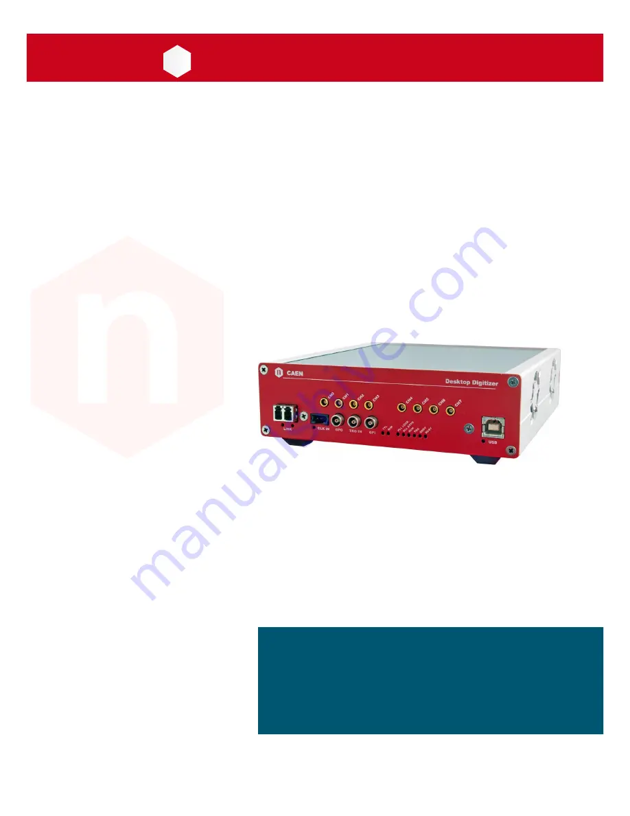
Page 10: ...box Fig 4 1 Front view CAUTION to manage the product consult the operating instructions provided A POTENTIAL RISK EXISTS IF THE OPERATING INSTRUCTIONS ARE NOT FOLLOWED CAEN provides the specific docu...
Page 11: ...with the digitizer and included in the delivered kit The DT5730 typical power consumption is 2 8 A 12 V Note Using a different power supply source like battery or linear type it is recommended the sou...
Page 12: ...CHIPS DURING THE BOARD OPERATION BY READING AT REGISTER ADDRESS 0x1nA8 The user can manually set the fan speed through the bit 3 at register address 0x8168 refer to RD2 Hardware revision 4 and ROC FPG...
Page 13: ...r temperature limit is fixed at 70 C As soon as the internal temperature exceeds 70 C the board enters the temperature protection condition and the firmware automatically performs the following action...
Page 14: ...CAEN Electronic Instrumentation UM3148 DT5730 DT5725 User Manual rev 2 14 8 Panels Description Fig 8 1 Front panel view Fig 8 2 Rear panel view...
Page 15: ...ectors Type CS 85MCX 50 0 16 Manufacturer SUHNER Suggested plug MCX 50 2 16 type Suggested cable RG174 type CLK IN FUNCTION Input connector for the external clock ELECTRICAL SPECS Sign type differenti...
Page 16: ...CAL SPECS Series 101 A 004 connectors Type DLP 101 A 004 28 Manufacturer FISCHER Alternatively Type EPL 00 250 NTN Manufacturer LEMO TRG IN FUNCTION Digital input connector for the external trigger EL...
Page 17: ...ECS Standard compliant to USB 2 0 and USB 1 0 Transfer rate up to 30 MB s MECHANICAL SPECS Series USB connectors Type 787780 2 B Type Manufacturer AMP Inc USB LINK LED GREEN indicates the USB communic...
Page 18: ...ternal AC DC adapter ELECTRICAL SPECS Typ Input voltage 12 VDC MECHANICAL SPECS Series CC power supply connectors Type RAPC722X DC power jack Manufacturer Switchcraft Inc PINOUT C ON OFF SWITCH FUNCTI...
Page 19: ...signal The input bandwidth ranges from DC to 250 MHz 3dB for DT5730 to 125 MHz 3dB for DT5725 by 2nd order linear phase anti aliasing low pass filter 1 00 0 2 00 1 00 2 00 Input Dynamic Range 2 Vpp Po...
Page 20: ...or 50 MHz or from external clock input By default the board uses the internal clock as PLL reference REF CLK The external clock can be selected by write access at register address 0x8100 refer to RD2...
Page 21: ...it 6 at register address 0x8100 must be set see RD2 3 External clock source different from 50 MHz In this case the user is required to program the AD9520 dividers in order to lock the VCXO to REF CLK...
Page 22: ...mance the calibration procedure is recommended to be executed by the user on command after the ADCs have stabilized their operating temperature The calibration will not need to be repeated at each run...
Page 23: ...required to calibrate after a board reset but if a Reset command is intentionally issued to the digitizer write access at register address 0xEF24 to be directly followed by a calibration procedure it...
Page 24: ...that the digitizer has been calibrated at least once NOTE THAT If SKIP_STARTUP_CALIBRATION parameter is set to YES in WaveDump configuration file the automatic start up calibration is not performed an...
Page 25: ...relevant column until you see they don t vary significantly 4 Go to the General tab and press the Calibrate button 5 Start the acquisition Fig 9 6 Channel calibration in DPP PSD Control Software MC2An...
Page 26: ...s stopped while bit 2 1 means running GPI CONTROLLED MODE bits 1 0 01 If the acquisition is armed i e bit 2 1 then Run starts when GPI is asserted and stops when GPI returns inactive If bit 2 0 the ac...
Page 27: ...epted programmable via software If the board is programmed to accept the overlapped triggers by programming at register address 0x8000 as the overlapping trigger arrives the current active buffer is f...
Page 28: ...s 640 samples in each buffer IMPORTANT For AMC FPGA firmware release 0 2 the Size of one Buffer related to each Buffer Number must be intended as the number of the samples in Tab 9 1 without decreasin...
Page 29: ...ovide different trigger information according to the setting of the bits 22 21 at register address 0x811C Tab 9 2 Note for ROC FPGA firmware revisions lower than 4 6 these bits are reserved REGISTER 0...
Page 30: ...ag specifications result in 16 ns resolution and 17 s range i e 8 ns 231 1 which can be extended to 625 h i e 8 ns 248 1 by the Extended Trigger Time Tag option Data are the samples from the enabled c...
Page 31: ...ew trigger This way the FULL reflects the BUSY condition of the board i e inability to accept triggers if required the BUSY signal can be provided out on the digitizer front panel through the GPO LEMO...
Page 32: ...s configurable at register address 0x810C Software trigger External trigger Self trigger Coincidence TRG IN Enable Mask x4 COMMON TRIGGER SW TRG GPO TRG OUT TRG_REQ 3 0 D Q SCLK Acquisition Logic Memo...
Page 33: ...matizes the self trigger and trigger request logic having the channel 0 and channel 1 couple as an example CH0 CH1 PULSE OVTHR Bits 1 0 of 0x1084 PULSE OVTHR SELF_TRG 0 SELF_TRG 1 AND ONLY 0 ONLY 1 OR...
Page 34: ...CH n ONLY CH n 1 OR of the relevant self trigger signals see Fig 9 10 Default Conditions by default the FPGA is programmed so that the trigger request is the OR of two pulses of 4ns width Note the abo...
Page 35: ...set the coincidence window TTVAW linearly in steps of the Trigger clock 8 ns Bits 26 24 set the Majority i e Coincidence level the coincidence takes place when Number of enabled trigger requests Majo...
Page 36: ...H1 THRESHOLD CH1 enabled IN Over threshold signal CH1 TRG_REQ 0 MEZZANINE CH2 THRESHOLD CH2 enabled IN Over threshold signal CH2 CH3 THRESHOLD CH3 enabled IN Over threshold signal CH3 TRG_REQ 1 Fig 9...
Page 37: ...d so that the relevant trigger requests are the over threshold signals from CH0 and CH1 CH2 THRESHOLD TRG_REQ 0 TRG_REQ 1 CH0 enabled IN CH0 THRESHOLD TRIGGER Maj lev 1 CH2 enabled IN ORed signal TTVA...
Page 38: ...sts are the over threshold signals from CH0 and CH1 CH2 THRESHOLD TRG_REQ 0 TRG_REQ 1 CH0 enabled IN CH0 THRESHOLD TRIGGER Maj lev 1 CH2 enabled IN ORed signal TTVAW MEZZANINE MOTHERBOARD Fig 9 16 Tri...
Page 39: ...other boards Thanks to its configurability see Fig 9 17 GPO can propagate out the OR of all the enabled trigger sources only the Software Trigger is provided by default as in the red path of Fig 9 17...
Page 40: ...ibed 1 Register 0x8110 on board n Enable the desired trigger request as Trigger Out signal on board n by bits 3 0 mask Disable Software Trigger and External Trigger as Trigger Out signal on board n bi...
Page 41: ...forms a FPGAs global reset which restores the FPGAs to the default configuration It initializes all counters to their initial state and clears all detected error conditions Memory Reset The Memory Res...
Page 42: ...pt to the PC over the optical communication link not supported by USB Using Polling interrupts disabled by performing periodic read accesses to a specific register of the board it is possible to know...
Page 43: ...3818 PCIe Optical Link Controller Detailed information on CAEN PCI PCIe Controllers can be find at www caen it Home Products Modular Pulse Processing Electronics PCI PCIe Optical Controllers The param...
Page 44: ...es and Controllers V1718 VX1718 VME USB2 0 Bridge V2718 VX2718 VME PCI PCIe Optical Link Bridge A2818 A3818 PCI PCIe CONET Controller The CAENVMElib installation package is available on CAEN website i...
Page 45: ...Tools USB 2 0 User s own SW DT5730 DT5725 CAENComm CAENDigitizer Library A2818 driver A3818 driver USB driver PCI PCIe Fig 10 1 Required libraries and drivers If required to be installed apart by the...
Page 46: ...ase of pay firmware Upgrade the internal PLL Get the Board Info file useful in case of support CAENUpgrader can operate with Windows and Linux 32 and 64 bit OSs The program relies on the CAENComm and...
Page 47: ...e access to the registers and may be used as a debug instrument Fig 11 2 CAENComm Demo Java and LabVIEW graphical interface CAENComm Demo can operate with Windows OSs 32 and 64 bit It requires CAENCom...
Page 48: ...anks to the included source files and the VS project starting with this demo is strongly recommended to all those users willing to write the software on their own Fig 11 3 CAEN WaveDump CAEN WaveDump...
Page 49: ...and restore the program settings Fig 11 4 CAENScope main frame CAENScope can operate with Windows and Linux 32 and 64 bit OSs Linux users are required to install the following packages sharutils libX...
Page 50: ...Software is available both for Windows and Linux platforms The program relies on the CAENDigitizer CAENComm and CAENVMELib libraries see 10 Third party Java SE6 or later needs to be installed Note Win...
Page 51: ...orms for on line monitoring of the acquisition and histograms It can also control the HV power supplies provided in the x780 Moreover it is able to perform advanced mathematical analysis on both the o...
Page 52: ...FF rear switch See Rear Panel to identify the relevant components Power on Status At power on the module is in the following status the Output Buffer is cleared registers are set to their default conf...
Page 53: ...le automatically loading the first working firmware copy that is the STD one by default It is possible to upgrade the board firmware via USB or Optical Link by writing the FLASH with the CAENUpgrader...
Page 54: ...digital trapezoidal filters The DPP PSD firmware updates are available for download on CAEN website in the Download tab login required at Home Products Firmware Software Digitizer Software Readout So...
Page 55: ...he Product Return Form PRF in the Returns and Repairs area at Home Support Services describing the specific failure A printed copy of the PRF must also be included in the package to be shipped Contact...
Page 56: ...s including engineers scientists and technical professionals who all trust them to help achieve their goals faster and more effectively CAEN S p A CAEN GmbH CAEN Technologies Inc Via Vetraia 11 Klinge...