


SLUS530D − SEPTEMBER 2002 − REVISED SEPTEMBER 2003
www.ti.com
13
FUNCTIONAL DESCRIPTION
After charge termination, the bqTINY restarts the charge once the voltage on the BAT pin falls below the V
(RCH)
threshold. This feature keeps the battery at full capacity at all times. Please see Battery Absent Detection section
for additional details.
SLEEP MODE
The bqTINY enters the low-power sleep mode if the V
CC
is removed from the circuit. This feature prevents draining
the battery during the absence of V
CC
.
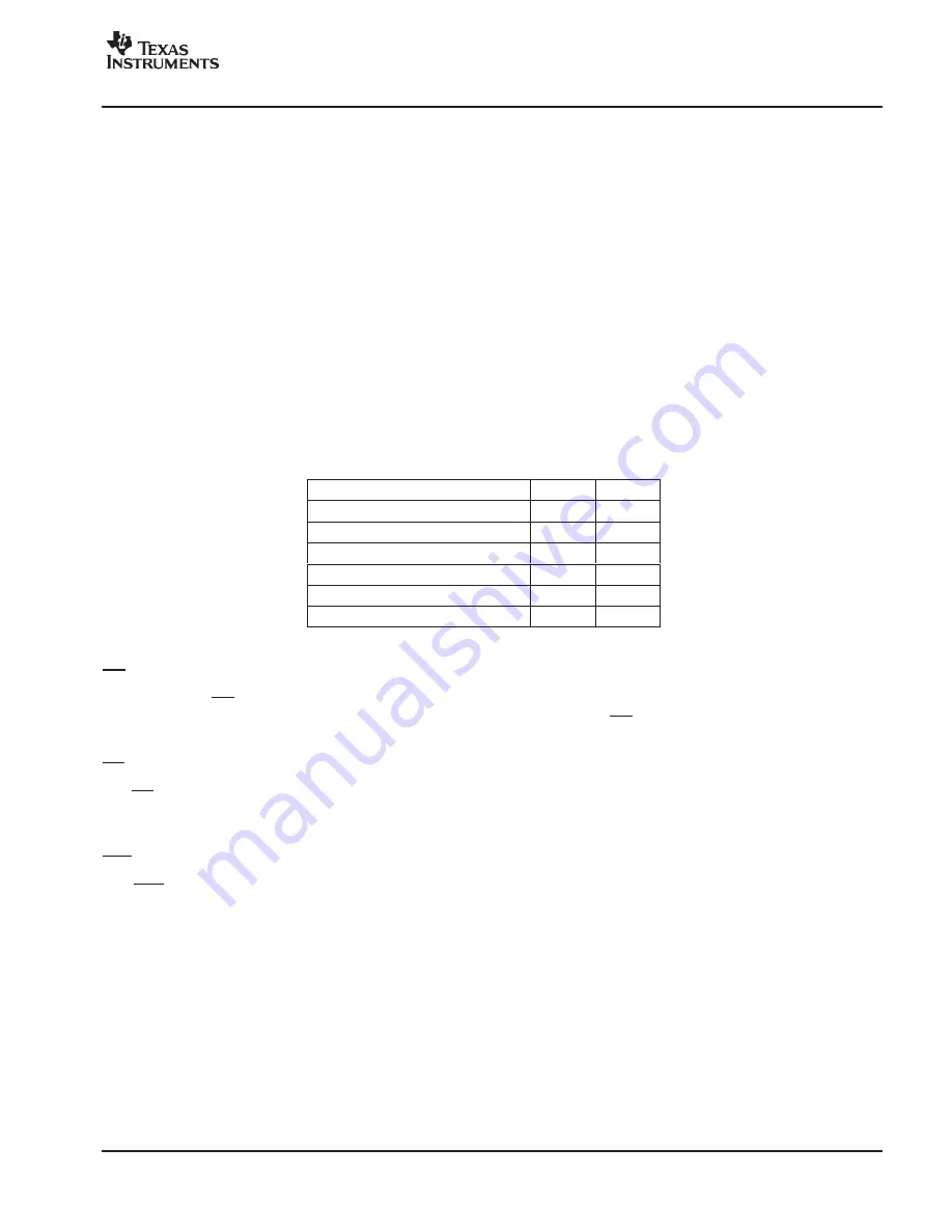
CHARGE STATUS OUTPUTS
The open-collector STAT1 and STAT2 outputs indicate various charger operations as shown in the following table.
These status pins can be used to drive LEDs or communicate to the host processor. Note that OFF indicates the
open-collector transistor is turned off.
Table 1. Status Pins Summary
CHARGE STATE
STAT1
STAT2
Battery absent
OFF(
)
OFF
Charge-in-progress
ON
OFF
Charge done
OFF
ON
Charge suspend (temperature)
OFF
OFF
Timer fault
OFF
OFF
Sleep mode
OFF
OFF
(
)
OFF means the open-collector output transistor on the STAT1
or STAT2 pins is in an off state.
PG OUTPUT
The open-drain PG (power good) indicates when the ac adapter (i.e. V
CC
) is present. The output turns ON when
a valid V
CC
is detected. This output is turned off in the sleep mode. The PG pin can be used to drive an LED or
communicate to the host processor.
CE INPUT (CHARGE ENABLE)
The CE digital input is used to disable or enable the charge process. A low-level signal on this pin enables the charge
and a high-level signal disables the charge. A high-to-low transition on this pin also resets all timers and fault
conditions and starts a new charge cycle.
TTE INPUT (TIMER AND TERMINATION ENABLE)
The TTE digital input is used to disable or enable the fast-charge timer and charge termination. A low-level signal
on this pin enables the fast-charge timer and termination and a high-level signal disables this feature. A high-to-low
transition on this pin also resets all timers.
THERMAL SHUTDOWN AND PROTECTION
The bqTINY monitors the junction temperature, T
J
, of the die and suspends charging if T
J
exceeds 155
C. Charging
resumes when T
J
falls below approximately 130
C.
Summary of Contents for PV420S
Page 1: ...SERVICE MANUAL PV420S WWW BBK RU ...
Page 72: ... 69 CXD3068Q Block Diagram ...
Page 73: ... 70 CXD3068Q Pin Configuration ...
Page 122: ... 119 CXD3068Q Timing Chart 1 3 ...
Page 123: ... 120 CXD3068Q Timing Chart 1 4 ...
Page 124: ... 121 CXD3068Q Timing Chart 1 5 ...
Page 129: ... 126 CXD3068Q Timing Chart 2 1 ...
Page 130: ... 127 CXD3068Q Block Diagram 2 2 ...
Page 131: ... 128 CXD3068Q Timing Chart 2 3 ...
Page 134: ... 131 CXD3068Q Timing Chart 2 6 ...
Page 138: ... 135 CXD3068Q VCO C Mode Fig 3 3 Access Flow Chart Using VCO Control ...
Page 140: ... 137 CXD3068Q Block Diagram 4 1 ...
Page 143: ... 140 CXD3068Q Timing Chart 4 4 ...
Page 147: ... 144 CXD3068Q Fig 4 6 a Auto Focus Flow Chart Fig 4 6 b Auto Focus Timing Chart ...
Page 148: ... 145 CXD3068Q Fig 4 7 a 1 Track Jump Flow Chart Fig 4 7 b 1 Track Jump Timing Chart ...
Page 149: ... 146 CXD3068Q Fig 4 8 a 10 Track Jump Flow Chart Fig 4 8 b 10 Track Jump Timing Chart ...
Page 150: ... 147 CXD3068Q Fig 4 9 a 2N Track Jump Flow Chart Fig 4 9 b 2N Track Jump Timing Chart ...
Page 151: ... 148 CXD3068Q Fig 4 10 a Fine Search Flow Chart Fig 4 10 b Fine Search Timing Chart ...
Page 152: ... 149 CXD3068Q Fig 4 11 a M Track Move Flow Chart Fig 4 11 b M Track Move Timing Chart ...
Page 157: ... 154 CXD3068Q Fig 4 15 CD TEXT Data Timing Chart ...
Page 162: ... 159 CXD3068Q Fig 5 3a Fig 5 3b ...
Page 196: ... 193 CXD3068Q Description of Data Readout ...
Page 200: ... 197 CXD3068Q ...
Page 201: ... 198 CXD3068Q ...
Page 202: ... 199 CXD3068Q ...
Page 207: ... 204 CXD3068Q Package Outline Unit mm ...
Page 208: ...This data sheet has been made from recycled paper to help protect the environment 205 ...


