


208
© 1999 Silicon Storage Technology, Inc.
336-04 1/99
2 Megabit Multi-Purpose Flash
SST39VF020
Preliminary Specifications
1
2
3
4
5
6
7
8
9
10
11
12
13
14
15
16
Toggle Bit (DQ
6
)
During the internal Program or Erase operation, any
consecutive attempts to read DQ
6
will produce alternat-
ing 0’s and 1’s, i.e., toggling between 0 and 1. When the
internal Program or Erase operation is completed, the
toggling will stop. The device is then ready for the next
operation. The Toggle Bit is valid after the rising edge of
fourth WE# (or CE#) pulse for Program operation. For
Sector or Chip Erase, the Toggle Bit is valid after the
rising edge of sixth WE# (or CE#) pulse. See Figure 7 for
Toggle Bit timing diagram and Figure 15 for a flowchart.
Data Protection
The SST39VF020 device provides both hardware and
software features to protect nonvolatile data from inad-
vertent writes.
Hardware Data Protection
Noise/Glitch Protection: A WE# or CE# pulse of less than
5 ns will not initiate a write cycle.
V
DD
Power Up/Down Detection: The Write operation is
inhibited when V
DD
is less than 1.5V.
Write Inhibit Mode: Forcing OE# low, CE# high, or WE#
high will inhibit the Write operation. This prevents inad-
vertent writes during power-up or power-down.
Software Data Protection (SDP)
The SST39VF020 provides the JEDEC approved soft-
ware data protection scheme for all data alteration op-
eration, i.e., program and erase. Any Program operation
requires the inclusion of a series of three byte sequence.
The three byte-load sequence is used to initiate the
Program operation, providing optimal protection from
inadvertent Write operations, e.g., during the system
power-up or power-down. Any Erase operation requires
the inclusion of six byte load sequence. The
SST39VF020 device is shipped with the software data
protection permanently enabled. See Table 4 for the
specific software command codes. During SDP com-
mand sequence, invalid commands will abort the device
to read mode, within T
RC
.
Product Identification
The product identification mode identifies the device as
the SST39VF020 and manufacturer as SST. This mode
may be accessed by hardware or software operations.
The hardware operation is typically used by a program-
mer to identify the correct algorithm for the SST39VF020
device. Users may wish to use the software product
identification operation to identify the part (i.e., using the
device code) when using multiple manufacturers in the
same socket. For details, see Table 3 for hardware
operation or Table 4 for software operation, Figure 10 for
the software ID entry and read timing diagram and Figure
16 for the ID entry command sequence flowchart.
Product Identification Mode Exit/Reset
In order to return to the standard read mode, the Soft-
ware Product Identification mode must be exited. Exiting
is accomplished by issuing the Exit ID command se-
quence, which returns the device to the Read operation.
Please note that the software reset command is ignored
during an internal Program or Erase operation. See
Table 4 for software command codes, Figure 11 for
timing waveform and Figure 16 for a flowchart.
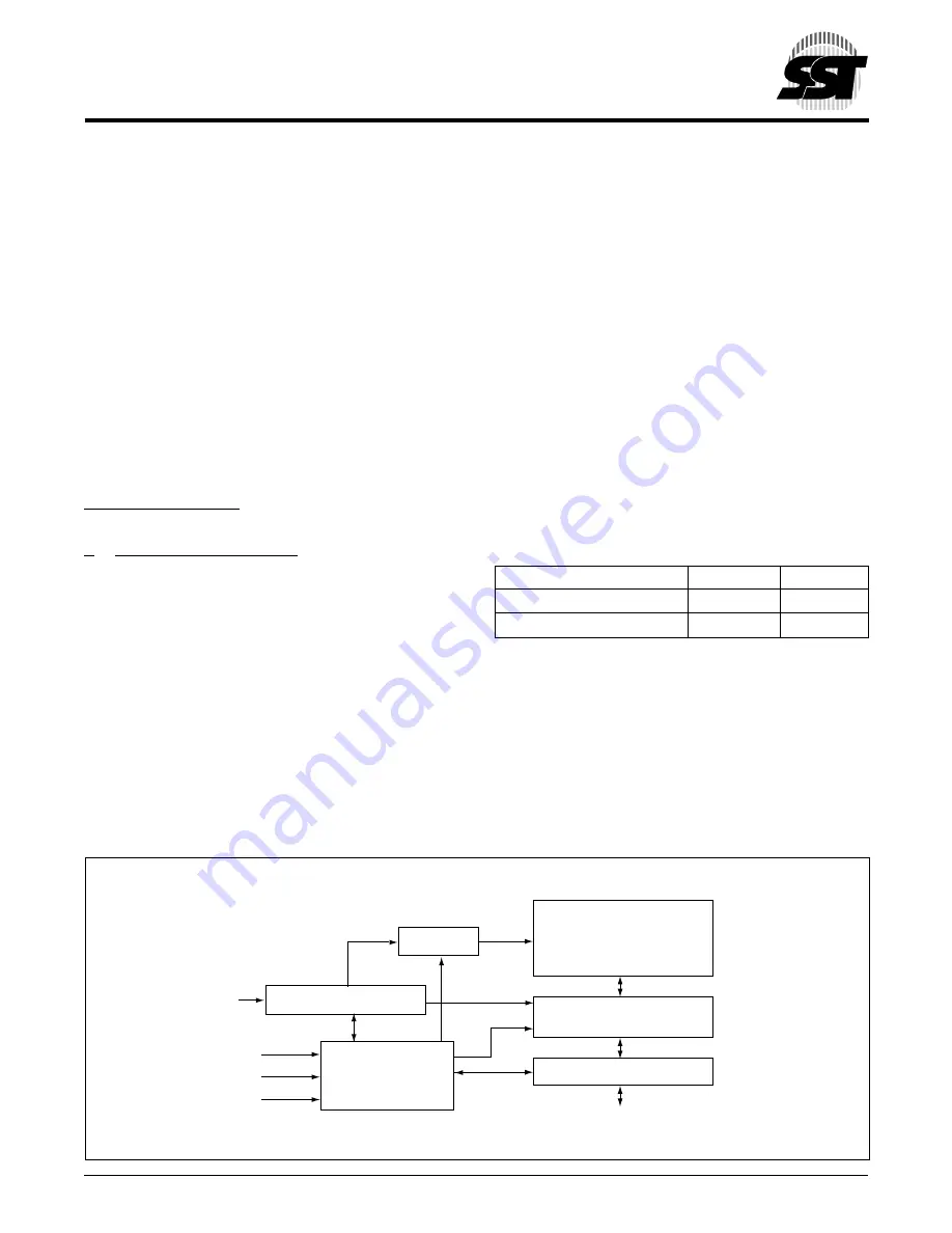
F
UNCTIONAL
B
LOCK
D
IAGRAM
OF
SST39VF020
T
ABLE
1: P
RODUCT
I
DENTIFICATION
T
ABLE
Address
Data
Manufacturer’s Code
0000H
BF H
Device Code
0001H
D6 H
336 PGM T1.0
Y-Decoder
I/O Buffers and Data Latches
336 ILL B1.0
Address Buffers & Latches
X-Decoder
DQ7 - DQ0
A17 - A0
OE#
CE#
WE#
2,097,152 bit
EEPROM
Cell Array
Control Logic
Summary of Contents for PV420S
Page 1: ...SERVICE MANUAL PV420S WWW BBK RU ...
Page 72: ... 69 CXD3068Q Block Diagram ...
Page 73: ... 70 CXD3068Q Pin Configuration ...
Page 122: ... 119 CXD3068Q Timing Chart 1 3 ...
Page 123: ... 120 CXD3068Q Timing Chart 1 4 ...
Page 124: ... 121 CXD3068Q Timing Chart 1 5 ...
Page 129: ... 126 CXD3068Q Timing Chart 2 1 ...
Page 130: ... 127 CXD3068Q Block Diagram 2 2 ...
Page 131: ... 128 CXD3068Q Timing Chart 2 3 ...
Page 134: ... 131 CXD3068Q Timing Chart 2 6 ...
Page 138: ... 135 CXD3068Q VCO C Mode Fig 3 3 Access Flow Chart Using VCO Control ...
Page 140: ... 137 CXD3068Q Block Diagram 4 1 ...
Page 143: ... 140 CXD3068Q Timing Chart 4 4 ...
Page 147: ... 144 CXD3068Q Fig 4 6 a Auto Focus Flow Chart Fig 4 6 b Auto Focus Timing Chart ...
Page 148: ... 145 CXD3068Q Fig 4 7 a 1 Track Jump Flow Chart Fig 4 7 b 1 Track Jump Timing Chart ...
Page 149: ... 146 CXD3068Q Fig 4 8 a 10 Track Jump Flow Chart Fig 4 8 b 10 Track Jump Timing Chart ...
Page 150: ... 147 CXD3068Q Fig 4 9 a 2N Track Jump Flow Chart Fig 4 9 b 2N Track Jump Timing Chart ...
Page 151: ... 148 CXD3068Q Fig 4 10 a Fine Search Flow Chart Fig 4 10 b Fine Search Timing Chart ...
Page 152: ... 149 CXD3068Q Fig 4 11 a M Track Move Flow Chart Fig 4 11 b M Track Move Timing Chart ...
Page 157: ... 154 CXD3068Q Fig 4 15 CD TEXT Data Timing Chart ...
Page 162: ... 159 CXD3068Q Fig 5 3a Fig 5 3b ...
Page 196: ... 193 CXD3068Q Description of Data Readout ...
Page 200: ... 197 CXD3068Q ...
Page 201: ... 198 CXD3068Q ...
Page 202: ... 199 CXD3068Q ...
Page 207: ... 204 CXD3068Q Package Outline Unit mm ...
Page 208: ...This data sheet has been made from recycled paper to help protect the environment 205 ...


