background image

– 160 –

CXD3068Q

§ 5-6. AGCNTL (Automatic Gain Control) Function

The AGCNTL function automatically adjusts the filter internal gain in order to obtain the appropriate servo loop

gain. AGCNTL not only copes with the sensitivity variation of the actuator and photo diode, etc., but also

obtains the optimal gain for each disc.

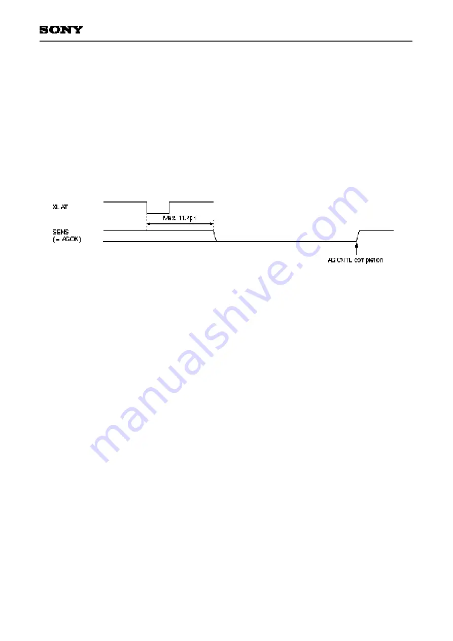
The AGCNTL command is sent when each servo is turned on. During AGCNTL operation, if the upper 8 bits of

the command register are 38 (Hex), the completion of AGCNTL operation can be confirmed by monitoring the

SENS pin. (See Timing Chart 5-4 and "Description of SENS Signals".)

Setting D9 and D8 of $38 to 1 set FCS (focus) and TRK (tracking) respectively to AGCNTL operation.

Note) During AGCNTL operation, each servo filter gain must be normal, and the anti-shock circuit (described

hereafter) must be disabled.

Timing Chart 5-4.

Coefficient K13 changes for AGF (focus AGCNTL) and coefficients K23 and K07 change for AGT (tracking

AGCNTL) due to AGCNTL.

These coefficients change from 01 to 7F (Hex), and they must also be set within this range when written

externally.

After AGCNTL operation has completed, these coefficient values can be confirmed by reading them out from

the SENS pin with the serial readout function (described hereafter).

AGCNTL related settings

The following settings can be changed with $35, $36 and $37.

FG6 to FG0; AGF convergence gain setting, effective setting range: 00 to 57 (Hex)

TG6 to TG0; AGT convergence gain setting, effective setting range: 00 to 57 (Hex)

AGS;

Self-stop on/off

AGJ;

Convergence completion judgment time

AGGF;

Internally generated sine wave amplitude (AGF)

AGGT;

Internally generated sine wave amplitude (AGT)

AGV1;

AGCNTL sensitivity 1 (during rough adjustment)

AGV2;

AGCNTL sensitivity 2 (during fine adjustment)

AGHS;

Rough adjustment on/off

AGHT;

Fine adjustment time

Note) Converging servo loop gain values can be changed with the FG6 to FG0 and TG6 to TG0 setting values. In

addition, these setting values must be within the effective setting range. The default settings aim for 0dB at

1kHz. However, since convergence values vary according to the characteristics of each constituent

element of the servo loop, FG and TG values should be set as necessary.

Summary of Contents for PV420S

Page 1: ...SERVICE MANUAL PV420S WWW BBK RU ...

Page 2: ...CHNICAL DATA 3 4 MM1538 DATA BOOK instead of FAN8038 31 5 CXA2550 DATA BOOK 55 6 CXD3068Q DATA BOOK 68 7 SST39VF020 DATA BOOK 206 8 SPCA717A DATA BOOK 229 9 BH3541F BH3544F DATA BOOK 257 10 BQ24010 DATA BOOK 265 11 Si2323 DATA BOOK instead of Si2305 286 12 SCHEMATIC DIAGRAM 289 ...

Page 3: ...rporates a digital servo MPEG The SPCA716A A V decoder is a single chip VCD decoder this LSI incorporates a MCU TV ENCODER The SPCA717A is a single chip VCD encoder D A The WM8714 is a digital to analog converter Power AMP The BH3544 is audio power AMP so that to driver headphone SPCA716A MPEG MCU CXD3068Q DSP CXA2550N RF AMP FAN8038 Driver WM8714 D A Converter DC DC Converter Dram 16M 4 SPCA717A ...

Page 4: ...SCOR CD_C2PO CD_SENS CD_CLOK CD_XLAT CD_DDAT CD_SQCK CD_SQSO CD_LRCK CD_DATA CD_BLCK RF_SPEED RF_LDON POW_STB OFF START BATT_DET SERVO SERVO PART POW_DET SCL SDA GR2003 1 SDA SCL START Line controler VID_RST VID_P N VID_CLK VID_VSYNC VID_HSYNC VID_D0 VID_D1 VID_D2 VID_D3 VID_D4 VID_D5 VID_D6 VID_D7 VIDEO SPCA717 POW_DET GR2003 2 PT9801 SCH VIDEO AUD_DEM AUD_BLCK AUD_LRCK AUD_DATA AUD_XCLK LOUT ROU...

Page 5: ... O R P O R A T I O N O P T I C A L D E V I C E D I V I S I O N MODEL 担 当 者 印 当該モデルの参考資料であり この資料の内容は将来変更する 可能性があります MODEL KSM1000BBC KSM1000BBC Sony reserves the right to change specification of products and discontinue products without notice PAGE 1 3 ...

Page 6: ... Specifications Optical Specifications Mechanical Specifications Electrical Specifications Of Pick up Evaluation Conditions Characteristics Specifications Absolute Maximum Rating Performance Specifications Reliability Standard Markings Attachment Description Of Components Appearance Drawing Pin Connection Diagram APC Circuit Diagram Standard Test Circuit Diagram Operating Voltage Range Position En...

Page 7: ...on デバイスをセットに実装した状態にてレーザー出力を測定して セットからの漏れ光が規制値を満足していることを確認して下さい Measure leak laser output from a finished product containing the device s and make sure that the finished product is in compliance with applicable requirements This document describes the specification of drive unit KSM1000BBC for use in compact disc player This model is not for professional use If any disagreement should arise these t...

Page 8: ...ltage applied to pin FCS of the flex moves the objective lens toward the disc トラッキング方向 Tracking Direction フレキ端子 トラッキンク にプラス電圧が印加された場合 対物レンズはディスクの内周方向に動く A positive voltage applied to pin TRK of the flex moves the objective lens toward the center of the disc 標準値 Standard value フォーカスエラー SSD法 トラッキングエラー 3スポット法 Focus error Tracking error 35g Figure 1 参照 3 SPOT method 4 対物レンズ可動範囲 Range of objective lens...

Page 9: ...へ動く A positive voltage applied to pin of sled motor moves the objective lens toward the outer of the disc ピックアップ可動範囲 Pick up movable distance 機械的内周位置 Mechanical center position 24 mm 機械的最外周位置 Mechanical the most periphery position 58 mm ターンテーブルセンターから対物レンズセンターまでの距離 Length between the center of turntable and objective lens ターンテーブル動作 Direction of turntable movement A positive voltage applied to pin o...

Page 10: ...onditions is acceptable 3 3 機 器 Equipment 測定用標準基台 Standard cabinet for measurement APC回路 Figure 4 APC circuit 標準評価回路 Figure 5 Standard measurement circuit ジッターメーター Jitter meter 菊水電子工業製 KJM 6235SA KJM 6235SA KIKUSUI ELE CO デジタルマルチメータ Digital multimeter サーボアナライザー Servo analyzer オシロスコープ Oscilloscope 3 4 ディスク Disc ソ ニー製ガラスディスク GLD CR11 Glass disc manufactured by SONY GLD CR11 温 度 Temperature 湿 度 Relat...

Page 11: ...s 電 源 電 圧 Supply Voltage 項 目 Item 規 格 備 考 Remarks 4 2 使用電圧範囲 Operating Voltage Range PDIC部 動作電源電圧 Vcc 中点電位電圧 Vc Operating supply voltage Vcc Neutral point voltage Vc 2 7 5 5 V 1 3 Vcc 1 3 V レーザーダイオード部 Laser diode PDIC部 項 目 Item 規 格 備 考 Remarks スピンド ル 送り モータ Spindle Sled motor 許容電圧 Allowable voltage スピンドル Spindle Focus Tracking total current must be less than 150mA RMS 6 V 送 り Sled 3 V Standard val...

Page 12: ...ture and humidity 温 度 変 化 Temperature Deviation Standard value 備 考 Remarks 6 1Ω mm V 46 7 Hz 12 5 6 dB 常 温 常 湿 6 3 1Ω mm V 46 8 Hz 14 5 6 dB 5 55 5Hzにて規定 Q値MAXにて規定 Q value Gain fo Gain 5Hz 5Hzにて規定 Q値MAXにて規定 Q value Gain fo Gain 5Hz Specified at 5Hz Specified at maximum Q value Specified at 5Hz Specified at maximum Q value Q 値 Q 値 1 ディスク上ビームスポットにて規定 Specified at beam spot on the disc 4 3 1 光学ピックアップ...

Page 13: ...合にジッター最良点 がある時 デフォーカスの極性はプラスといい 逆の場合をマイナスと規定する When objective lens moves toward the disc and able to get minimum jitter it is defined as plus otherwise it is defined as minus デフォーカス Defocus 0 1 2μm以内 within 極 性 Polarity or less F E オフセット レーザーON ディスクからの 戻り光が無い状態での フォーカスエラーのDCオフセット Focus error DC off set at laser on and no reflection from the disc APC temperature characteristics excluded RF 信号振...

Page 14: ...ck the direction toward the center of the disc is defined as plus and the periphery of the disc is defined as minus Disc rotating direction 内周側 外周側 ディスク 回転方向 トラッキングエラー信号 Polarity center periphery E F位相差 E F phase difference 60 以内 within トラッキングエラー信号振幅 Tracking error signal amplitude 0 30 以内 Tracking error signal 30 以内 within 30 以内 within 規 格 Room temperature and humidity 温 度 変 化 Temperature Deviat...

Page 15: ...tage Full stroke time Current consumption Make position of limit switch 1 0 V 以下 2 3 s 以下 160mA 以下 or less 印加電圧 1 5V 片道 印加電圧 1 5V Applied voltage 1 5V one way Applied voltage 1 5V ピックアップが機械的最内周位置に 達する前にメイクしていること Make should be completed before pick up operation reaches mechanically innermost position From insulator fixing surface or more Standard value or less or less 規 格 Room temperature and humi...

Page 16: ...bility specifications Do not let condensation to form on the mechanism 高温高湿保存 Storage in hot and humid conditions 上記環境に48h放置し 常温に戻して16h以上放置後の初期値に対する 特性変化は 信頼性保証規格の範囲内とする 但し 結露させないこと Leave the pick up at temperatures in the above range for 48 hours and then at room temperature for over 16 hours After the test the deviation of characteristics from the standard values must be within the tolerance spe...

Page 17: ... 10 000サイクル動作後 送りモータの消費電流は 初期値 30 以下 1サイクル 最内周 最外周 最内周 The current consumption of sled motor must be less than initial value plus 30 after 10 000 cycles 1cycle innermost track outermost track innermost track リミットスイッチ寿命 Service life of limit switch 10 000サイクル動作後 接触抵抗は500mΩ以下 The contact resistance must be less than 500mΩ after 10 000 cycles 1cycle innermost track outermost track innermost track ピック...

Page 18: ... 6 dB 光学部 Optics Standard value Deviations after evaluation tests under the conditions specified on reliability test except operating temperature test Actually measured value 項 目 Item 規 格 RF信号振幅 RF signal Amplitude ジッター Jitter フォーカスエラー信号振幅 Focus error signal amplitude RF信号 フォーカス信号 RF signal Focus signal デフォーカス Defocus トラバース信号 Traverse signal EFバランス EF balance トラッキングエラー信号振幅Tracing error signal am...

Page 19: ...000BBC 15 送り機構部 項 目 Item 規 格 Sled mechanism 最低起動電圧 送り時間 消費電流 Minimum starting voltage Sled time Current consumption 1 2 V 以下 3 sec 以下 or less or less 210 mA 以下 or less 印加電圧 1 5 V Applied voltage 1 5V 備 考 Remarks Standard value 17 ...

Page 20: ...nents Fig 1の各部名称参照 Lot No 日 月 西暦年号の末尾 品質管理No Day Month Last digit of year Quality control No 但し 月表示の10 11 12はX Y Zで表わす X Y and Z signify October November and December respectively 英字又は数字 Alphabet or Number The last alphabet is for management purposes in the factory Use up to three characters 末尾の英字は 製造所の管理に用いる場合がある 但し 桁数は0 3桁迄とする 18 ...

Page 21: ...fications 本機種を保護シートに入れる Set into protection sheet Set into MD case 50 pcs 2 lines Total 100 pcs MDケースに100個 50 2列 収納する 保護シート Protection sheet MDカバー MD cover MDケース MD case MD cover MDケース MD case マスターカートン Master carton PPテープ PP tape 出荷ラベル Shipping label MDカバー 19 ...

Page 22: ...ODEL KSM1000BBC X軸 axis Y軸 axis 8 付 図 Attachment Figure 1 各部の名称 Description of components 18 光学ピックアップ Optical pick up ターンテーブル Turntable Z軸 axis 機種名 Lot No 捺印箇所 Stamping area of Model name and Lot NO MDシャーシ MD chassis 20 ...

Page 23: ...PAGE MODEL KSM1000BBC FO OP 94094 19 Figure 2 外形図 Appearance Drawing Note 1 Recommended FPC position 注1 推奨フレキ位置 To the bottom of chassis To the bottom of motor Note 1 General Tolerance 0 3 一般公差 0 3 21 ...

Page 24: ...mended connector Product of ELCO INTERNATIONAL CO LTD Series 6224 推奨コネクター 日本圧着端子Z R シリーズ Recommended connector Product of JAPAN SOLDERLESS TERMINAL CO LTD Series ZR SPINDLE SLD Mo SP Mo フォーカスエラー 信号 PD1 PD2 トラッキングエラー信号 E F RF 信号 PD1 PD2 LIMIT SW LIMIT SW LIMIT SW ピンNo Pin No 1 2 3 4 5 6 7 8 9 10 11 12 13 14 15 16 端子名称 Terminal E Vcc GND Vcc PD2 LD GND LD VR Mon out PD1 VC F GND PDIC FCS TRK TRK FCS...

Page 25: ...PAGE MODEL KSM1000BBC FO OP 94094 21 Figure 4 APC回路参考図 IC CXA 1081M TR1 2SB731 D1 1S1555 APC Circuit diagram Reference 23 ...

Page 26: ...PAGE MODEL KSM1000BBC FO OP 94094 22 Figure 5 標準評価回路図 Standard test circuit diagram 18k PD1 18k PD1 PD2 PD2 2 PD1 PD2 470k 150k 150k 470k 470k 150k 150k 470k PD1 PD2 PD1 PD2 PD1 10k PD2 2 24 ...

Page 27: ...range between motor terminals DC Rated load Speed Current Initial torque Initial current At rated voltage and load At rated voltage and load At rated voltage and by winding up method At rated voltage 2 0 V 1 0 3 0 V 0 49 mN m 2300 345 r min 145 mA 以下 1 37 mN m 以上 400 mA 以下 Standard operating conditions and electrical characteristics for reference モータ特性図 Motor characteristics diagram or less or les...

Page 28: ...使用電圧範囲 モータ端子間 DC 定格負荷 定格負荷回転数 定格負荷電流 始動トルク 始動電流 定格電圧 定格負荷にて 定格電圧 定格負荷にて 定格電圧 2点法 定格電圧にて Rated voltage DC Used voltage range between motor terminals DC Rated load Speed Current Initial torque Initial current At rated voltage and load At rated voltage and load At rated voltage Standard operating conditions Electrical characteristics At rated voltage and by 2points 1 5 VDC 1 5 3 0 V 0 0981 mN m 180 m...

Page 29: ...nt RF level will be 1 Vp p when the attached standard test circuit is used 結 線 Connections 結線は 必らず指定形状のフレキシブル基板を使用してください フォトダイオードからのハーネス近くにマイコン等のデジタルノイズ源が 有りますと アイパターンが劣化することが有りますので注意して下さい 2軸 レーザーダイオードコネクターに関する結線に接触不良が有りますと レーザー劣化の原因となりますので コネクター等のゆるみがないように して下さい Use the specified connectors for electrical connections The eye pattern may deteriorate if a digital noise source such as a microcompute...

Page 30: ...し酸やアルカリへ 入れたり 200 以上に加熱したり 口に入れたりすることは絶対に行わない で下さい ライン不良 サービスパーツの不良品は 廃棄物入れにまとめて 入れ 御社指定の方法で廃棄処理をして下さい The output from the LD is only 1mW maximum after going through the objective lens However the intensity of the focused beam reaches about 0 7 104 W cm2 Never look directly into the LD or observe the laser beam through another lens or mirror If you need to view the beam use an infrared viewer or a...

Page 31: ...insertion unstrap the LD terminal with a soldering iron with its metallic tip grounded or worse insulation resistance is 10 megohms or more at 500V DC five minutes after it is tuned on The temperature of the soldering iron tip must be 320 or below 30W and the unstrapping should be performed quickly 2軸部 Actuator アクチュエータ Actuator アクチュエータ部は強力な磁気回路を有していますので 磁性体が近づきすぎ ますと特性が変化します 又 すきまから異物が入ることの無いようにして...

Page 32: ...t approved as a unit Therefore apply for approval after mounting the optical drive unit in a player and check it for safety after mounting too Parts Name Material Manufacturer Grade Generic Name Type No ID Mark 光学ピックアップ部 Optical Pick up ドライブユニット部 Drive unit Parts Name Material Manufacturer Grade Generic Name Type No ID Mark 94V 1 ASAHI KASEI CORP PPE L543V MDシャーシ MD Chassis HOEフレキシブル基板 HOE FPC スラ...

Page 33: ...ets Features 1 Built in 4ch H bridge driver and PWM control of load drive voltage is made possible by external components 2 DC DC converter control circuit on chip 3 With reset output inversion output pin 4 Empty detection level can be switched between rechargeable battery and dry battery 5 Constant current charging current value can be varied using external resistor 6 Built in power transistor fo...

Page 34: ...K START OFF CHGVcc SEL PREGND PWMFIL IN1 MUTE2 IN2 MUTE34 IN4 IN3 Vref VSYS2 OP OPOUT VSYS1 RCHG OUTIR OUT1F OUT2R OUT2F POWGND OUT3F OUT3R OUT4F OUT4R BRAKE1 BSEN BATT RESET DEAD SW EO EI SPRT CT N C OP V I V I V I V I BRAKE1 BTL BTL BTL BTL POWER OFF STARTER MAXIMUM DETECTION CLK TSD TRIANGLE WAVE OVER VOLTAGE PRE DRIVER POWER SUPPLY TSD POWER UNIT POWER SUPPLY CONTROL CIRCUIT POWER SUPPLY MUTE2...

Page 35: ...0 MM1538XQ 29 27 26 25 24 23 28 EMP HVCC PSW CLK START OFF CHGVCC SEL PREGND PWMFIL IN1 MUTE2 IN2 MUTE34 IN4 IN3 Vref VSYS2 OP OPOUT VSYS1 1 BSEN 23 BRAKE1 2 BATT 24 OUT4R 3 RESET 25 OUT4F 4 DEAD 26 OUT3R 5 SW 27 OUT3F 6 EO 28 POWGND 7 EI 29 OUT2F 8 SPRT 30 OUT2R 9 CT 31 OUT1F 10 N C 32 OUT4R 11 OP 33 RCHG 12 VSYS1 34 AMUTE 13 OPOUT 35 EMP 14 OP 36 HVCC 15 VSYS2 37 PSW 16 Vref 38 CLK 17 IN3 39 STA...

Page 36: ...oltage Monitor 1 71kΩ 16 5kΩ 20kΩ 10 5kΩ 14 85kΩ Pin Description 5 150Ω 6kΩ BATT Input Battery Power Supply Input Input Power Supply 3 RESET Output Reset Detect Output 4 49kΩ 13kΩ 30 8kΩ 4 DEAD Input DEAD Time Setting 5 SW Output Transistor Drive For Voltage Multiplier 3 90kΩ VSYS1 2 BATT 6 VSYS1 6 EO Output Error Amplifier Output 34 ...

Page 37: ...6kΩ 7 VSYS1 Pin Description 14 11 Input Short Circuit Protection Setting Output 9 CT Output Triangular Wave Output 10 N C 11 OP 14 OP Input Op Amp Negative Input Op Amp Positive Input 420kΩ 10kΩ 2kΩ 9 VSYS1 BATT 8 SPRT 220kΩ 8 VSYS1 12 VSYS1 Input Control Circuit Power Supply Input Control Circuit Power Supply 13 VSYS1 13 OPOUT Output Op Amp Output 35 ...

Page 38: ...9 21 23 19 MUTE34 21 MUTE2 23 BRAKE1 Input ch3 and 4 Mute ch2 Mute ch1 Brake 11kΩ 20PIN 7 5kΩ 17 18 20 22 16 Vref 16 24kΩ 50kΩ 200Ω 4 36 24 26 30 32 25 27 29 31 28 24 OUT4R 25 OUT4F 26 OUT3R 27 OUT3F 29 OUT2F 30 OUT2R 31 OUT1F 32 OUT1R Output ch4 Negative Output ch4 Positive Output ch3 Negative Output ch3 Positive Output ch2 Positive Output ch2 Negative Output ch1 Positive Output ch1 Negative Outp...

Page 39: ...ut 34 95kΩ BATT Pin Description 39 390kΩ 200kΩ BATT Output Empty Detect Output Output 37 PSW Output PWM Transistor Drive 38 2kΩ 50kΩ 100kΩ VSYS1 38 CLK Input External Clock Synchronizing Input 39 START Input Voltage Multiplier DC DC Converter Start 50Ω 37 BATT 35 EMP 35 40 180kΩ 27kΩ VSYS1 40 OFF Input Voltage Multiplier DC DC Converter OFF 37 ...

Page 40: ...er Supply Input Pin Description Input Empty Detect Level Switch Input Output 43 PREGND Pre Section Power Supply Ground 2kΩ 2kΩ VSYS1 44 44 PWMFIL Input PWM Phase Compensation 42 SEL 200kΩ 130kΩ 15kΩ 42 BATT Charging Circuit Power Supply Pre Section Power Supply Ground The positive and negative outputs are the polarity with respect to the input 38 ...

Page 41: ... ICGVCC CHGVCC 4 5V ROUT OPEN 0 65 2 00 mA H Bridge Driver Part Voltage Gain ch1 ch3 ch4 GVC134 12 14 16 dB Voltage Gain ch2 GVC2 21 5 23 5 24 5 dB Gain Error By Polarity GVC 2 0 2 dB Input pin resistance ch1 ch3 ch4 RIN134 IN 1 7V and 1 8V 9 11 13 kΩ Input pin resistance ch2 RIN2 IN 1 7V and 1 8V 6 7 5 9 kΩ Maximum Output Voltage VOUT RL 8Ω HVcc BATT 4 0V IN 0 3 2V 1 9 2 1 V Saturation Voltage Lo...

Page 42: ... 0 0 1 V EO H SPRT Pin Current1 ISPR1 EI 0 7V 6 10 16 µA OFF L SPRT Pin Current2 ISPR2 EI 1 3V OFF 0V 12 20 32 µA SPRT Pin Current3 Over Voltage ISPR3 EI 1 3V BATT 9 5V 12 20 32 µA SPRT Pin Impedance RSPR 175 220 265 kΩ SPRT Pin Threshold Voltage VSPTH EI 0 7V CT 0V 1 10 1 20 1 30 V Over Voltage Protection Detect VHVPR BSEN Pin Voltage 8 0 8 4 9 0 V Transistor Driving SW Pin Output Voltage1 H VSW1...

Page 43: ...N 1V 0 5 V EMP Pin Output Leak Current IEMPL BSEN 2 4V 1 0 µA BSEN Pin Input Resistance RBSEN VSEL 0V 17 23 27 kΩ BSEN Pin Leak Current IBSENL VSYS1 VSYS2 0V BSEN 4 5V 1 0 µA SEL Pin Detection Voltage VSELTH VSELTH BATT SEL BSEN 2 0V 1 5 V SEL Pin Detection Current ISELT 2 µA Reset Circuit VSYS1 RESET Threshold Voltage Ratio HSRT Comparison with error amplifier threshold voltage 85 90 95 RESET Det...

Page 44: ...HVcc PSW CLK START OFF CHGVCC SEL PREGND PWMFIL RCHG OUT1R OUT1F OUT2R OUT2F POWGND OUT3F OUT3R OUT4F OUT4R BRAKE1 33 32 31 30 29 28 27 26 25 24 23 34 35 36 37 38 39 40 41 42 43 44 1 2 3 4 5 6 7 8 9 10 11 22 21 20 19 18 17 16 15 14 13 12 IN1 MUTE2 IN2 MUTE34 IN4 IN3 Vref VSYS2 OP OPOUT VSYS1 MM1538XQ BSEN BATT RESET DEAD SW EO EI SPRT Ct N C OP A V V A A V A V A V V V A A A V V A A V V V V A a a a...

Page 45: ...ltage a a SPRT Pin Current1 EO H a b SPRT Pin Current2 OFF L a b a SPRT Pin Current3 Over Voltage a a b SPRT Pin Impedance b SPRT Pin Threshold Voltage a a a Over Voltage Protection Detect a a SW Pin Output Voltage1 H a a a SW Pin Output Voltage2 H a a b a SW Pin Output Voltage2 L a a SW Pin Oscillating Frequency 1 b b a SW Pin Oscillating Frequency 2 b b b SW Pin Oscillating Frequency 3 b b a SW ...

Page 46: ... Voltage a a a START Pin Bias Current a CLK Pin Threshold Voltage H a b b CLK Pin Threshold Voltage L a b b CLK Pin Bias Current a Starter Switching Voltage a a Starter Switching Hysteresis Width a a Discharge Release Voltage a VSYS1 Pin RESET Threshold b Voltage Ratio RESET Detection Hysteresis Width b RESET Pin Output voltage b RESET Pin PULL UP Resistance a AMUTE Pin Output Voltage 1 b AMUTE Pi...

Page 47: ... Hysteresis Voltage 2 a a b EMP Pin Output Voltage a b EMP Pin Output Leak Current a c BSEN Pin Input Resistance a a BSEN Pin Leak Current a SEL Pin Detection Voltage a a a SEL Pin Detection Current a a b Input Bias Current a Input Offset Voltage d H Level Output Voltage b c L Level Output Voltage a c Output Drive Current Source d b Output Drive Current Sink d a Open Loop Voltage Gain b a Slew Rat...

Page 48: ... b b a ch1R b b b a Maximum Output Voltage ch2R b b b a ch3R b b b a ch4R b b b a ch1F b a a ch1R b a a ch2F b a a Saturation Voltage Lower ch2R b a a ch3F b a a ch3R b a a ch4F b a a ch4R b a a ch1F b a a ch1R b a a ch2F b a a Saturation Voltage Upper ch2R b a a ch3F b a a ch3R b a a ch4F b a a ch4R b a a ch1 a a Input Offset Voltage ch2 a a ch3 a a ch4 a a ch1 b b b a Output Offset Voltage ch2 b...

Page 49: ...8 BRAKE1 ON Voltage ch1 b b b a BRAKE1 OFF Voltage ch1 b b b a MUTE2 ON Voltage ch2 b b b a MUTE2 OFF Voltage ch2 b b b a MUTE34 ON Voltage ch3 b b b a ch4 b b b a MUTE34 OFF Voltage ch3 b b b a ch4 b b b a ch1 b b b a Vref ON Voltage ch2 b b b a ch3 b b b a ch4 b b b a ch1 b b b a Vref OFF Voltage ch2 b b b a ch3 b b b a ch4 b b b a BREAK1 Brake Current ch1 b b b a PWM Sink Current b a b a HVCC L...

Page 50: ...VIN1 VIN3 VO2 VO1 Dead Zone Output Offset Voltage VIN4 VIN2 XC XC Output voltage VO mV Input voltage V IN mV Voltage Gain GVC 20 log VO1 VO2 VIN1 VIN2 GVC 20 log VO3 VO4 VIN3 VIN4 Gain Error By Polarity GVC GVC GVC Dead Zone XC XC VIN2 VO1 VIN1 VO2 VIN3 VO4 VIN4 VO3 VO1 VO2 VO3 VO4 48 ...

Page 51: ...IRCUIT POWER SUPPLY RCHG OUTIR OUT1F OUT2R OUT2F POWGND OUT3F OUT3R OUT4F OUT4R BRAKE1 BSEN BATT RESET DEAD SW EO EI SPRT C T N C OP TRAVERSE SPINDLE FOCUS TRACKING BTL BTL BTL BTL MUTE2 MUTE34 FILTER 1 8k 0 1µ 470p 0 022µ 8 2k 100µ 0 1µ VOUT 47µ VIN 10p 2200p 100k 100k DC DC Converter application We shall not be liable for any trouble or damege caused by using this circuit In the event a problem ...

Page 52: ...brake mode When MUTE2 21PIN is set to high level the ch2 output is muted When MUTE34 19PIN is set to high level the ch3 and 4 outputs are muted 3 Vref drop mute When the voltage applied to Vref 16PIN is 1 0V or less typ the driver outputs are set to high impedance 4 Thermal shutdown When the chip temperature reaches 150 C typ the output current is cut The chip starts operating again at about 120 C...

Page 53: ...tching stops is set by the capacitor connected to SPRT 8PIN according to the following formula t CSPRT VTH sec VTH 1 2V ISPRT 10µA ISPRT 3 Soft start function The soft start function operates when a capacitor is connected between DEAD 4PIN and GND Also the maximum duty can be varied by connecting a resistor to 4PIN t CDEAD R sec R 65kΩ 4 Power off function When low level is applied to OFF 40PIN SP...

Page 54: ...nt output chattering Use SEL 42PIN to switch the detection voltage as shown below 5 Reset circuit block At about 90 typ of the DC DC converter output voltage RESET 3PIN goes from low level to high level and AMUTE 34PIN goes from high level to low level The reset voltage has 50mV typ of hysteresis to prevent output chattering 6 Charging circuit block The power supply for the charging circuit block ...

Page 55: ...oltage V O V Input voltage VIN V 3 2 1 0 1 2 3 0 8 0 6 0 4 0 2 0 0 2 20Ω RL Ta normal temperature BATT HVCC 4V VSYS1 VSYS2 3 2V Vref 1 6V 8Ω 4Ω 4Ω 8Ω 20Ω 0 8 0 4 0 6 Output voltage V O V Out voltage VO mV 0 006 0 004 0 002 0 0 002 0 004 0 006 30 20 10 0 10 20Ω Ta normal temperature BATT HVCC 4V VSYS1 VSYS2 3 2V Vref 1 6V 8Ω 4Ω 4Ω 8Ω 20Ω 30 20 Input voltage V IN mV Input Load Fluctuation Input Load...

Page 56: ... 5 1 0 1 5 2 0 2 5 Ta normal temperature BATT 2 4V EO PIN DAED PIN 4 0 3 0 3 5 Dead Output voltageE V DAED V Eo Output voltage V EO V Control Circuit Power Supply voltage VSYS1 V 4 5 4 0 3 5 3 0 2 5 2 0 1 5 1 0 0 5 0 0 0 5 1 0 1 5 2 0 2 5 Ta normal temperature BATT 2 4V 4 0 3 0 3 5 Reset Output voltage V RST V Error Amp Output Voltage Resete Pin Voltage 54 ...

Page 57: ... reserves the right to change products and specifications without prior notice This information does not convey any license by any implication or otherwise under any patents or other right Application circuits shown if any are typical examples illustrating the operation of the devices Sony cannot assume responsibility for any problems arising out of the use of these circuits CXA2550M 20 pin SOP Pl...

Page 58: ...rence level can be varied by the external resistor 147 13 4k 50µ 10µ 1 2 LD O APC amplifier output pin 4 5 PD1 PD2 I I Inversion input pin for RF I V amplifiers Connect these pins to the photodiodes A C and B D respectively The current is supplied 2 10k 1k 3 PD I APC amplifier input pin 55k 147 3 10k 20µ 8µ 10k 4 5 100µ 6 VEE 6 VEE VEE pin 56 ...

Page 59: ...p 9 EI Gain adjustment pin for I V amplifier 11 TE O Tracking error amplifier output pin E F signal is output 147 260k 26k 13k 9 10 VC O DC voltage output pin of Vcc VEE 2 Connect to GND for 1 75 power supply connect a smoothing capacitor for single 3 5V power supply 50 200µ 10 120 120 16k VCC VCC 15k VEE 96k 300µ 11 Pin No Symbol I O Equivalent circuit Description 57 ...

Page 60: ...2 13 FE O Focus error amplifier output pin 15 RF O O RF amplifier output pin 174k 300µ 13 24p 14 RFM I RF amplifier inverted side input pin RF amplifier gain is determined by the resistor connected between this pin and RFO pin 2k 1m 2k 147 850 14 15 147 60k 1m Pin No Symbol I O Equivalent circuit Description 58 ...

Page 61: ...n for RF level control 19 LD_ON I APC amplifier ON OFF switching pin OFF for Vcc and ON for VEE 147 50µ 10µ 17 50µ 18 AGCCONT I RF level control ON limit level of 50 30 OFF switching pin OFF for Vcc 30 for open or Vc and 50 for VEE 147 50k 15µ 15µ 7µ 18 147 50µ VREF 19 20 VCC VCC 20 Vcc pin Pin No Symbol I O Equivalent circuit Description ...

Page 62: ...Voltage gain 1 Voltage gain 2 Voltage gain difference Maximum output amplitude H Maximum output amplitude L Output voltage 1 Output voltage 2 Output voltage 3 Maximum output amplitude I CC I EE V15 1 V15 2 V15 3 V15 4 V15 5 V13 1 V13 2 V13 3 V13 4 V13 5 V13 6 V11 1 V11 2 V11 3 V11 4 V11 5 V11 6 V2 1 V2 2 V2 3 V2 5 O O O O O O O O O O O O O O O O O O O O O O O 0 8mA 450µA 570µA 0µA 0µA 300mV 300mV ...

Page 63: ... limit 50 limit 30 limit High Level Middle Level Low Level V2 7 V2 8 V2 9 V2 10 V18 1 V18 2 V18 3 V10 1 O O O O O O O O O 800µA 700µA 230µA 320µA 50mV 50mV 800mV 800mV 0 5V 2 7V 1 3V 2 7V 0 5V 2 7V 2 2V 2 7V 2 0V 2 0V 2 0V 2 0V 2 2 2 2 18 18 18 10 RF level control AGCCONT Output DC measurement I1 I2 E1 Center output voltage Level control 50 Level control OFF Level control 30 Level control OFF Leve...

Page 64: ... R5 390k S5 S6 AC E1 GND GND GND GND V EE V EE V CC V CC V EE GND R9 5 5k R10 10k GND R8 10k GND R7 10k GND R6 10k GND GND S8 E2 V EE R11 1M C2 0 1µ V EE E3 V EE E4 V EE C3 33µ GND 2 3 4 5 6 7 8 9 10 11 12 13 14 15 16 17 18 19 20 1 V CC AGCVTH LD_ON LD AGCCONT PD RFTC PD1 RF I PD2 RF O V EE RFM F FE E FE_BIAS EI TE VC S7 ...

Page 65: ...onse of the RF output signal can be equalized by adding the capacitance Cp to RFI pin The low frequency component of the RFO output voltage is as follows VRFO 2 75 VA VB 159 5kΩ iPD1 iPD2 Focus Error Amplifier The difference between the RF I V amplifier output VA and VB is obtained and the I V converted voltage of the photodiode A C B D is output The FE output voltage low frequency is as follows V...

Page 66: ...esistance value of the feedback resistors which are T type configured at the E I V amplifier by using the external resistance value of EI pin F I V amplifier feedback resistance value RF1 RF2 403kΩ E I V amplifier feedback resistance value RE1 R1 RE2 Leave EI pin open when the balance adjustment is not executed in this IC The gain for F I V and E I V amplifiers becomes the same when EI pin is left...

Page 67: ...he APC circuit is used to maintain the optical power output at a constant level The laser diode current is controlled according to the monitor photo diode output APC is set to ON by connecting the LD_ON pin to VCC OFF by connecting it to VCC VR 10 30k 30k VEE VCC 50 15 16 1 VEE VCC LD R1 22 C2 100µ L1 10µH LD PD C1 1µ GND R3 100 R2 500 PD R4 10k R5 55k R8 10k VEE 130mV R10 56k VCC R11 10k R12 56k ...

Page 68: ...TRK E GAIN I_V I_V I_V SSP GND 47k V CC SSP SSP R9 5 5k 0 01µ GND C3 0 1µ R11 1M MICRO COMPUTER MICRO COMPUTER 3 5V V CC 33µ 6 3V GND VC R5 270k 22k R5 4 7k VC GND R5 220k E F R4 220k GND VC 33µ 6 3V R3 33k R2 33k A B C D PD 500 100 LD 1µ 6 3V 10µH 11 100µ 6 3V V CC GND AGCVTH LD PD PD1 PD2 V EE F E EI VC V CC LD_ON AGCCONT RFTC RF I RF O RFM FE FE_BIAS TE FOCUS BIAS I_V TRK E GAIN I_V I_V I_V SSP...

Page 69: ...XA2550M N can be used either at dual power supply or single power supply The table below shows the connection of power supply for each case 2 RF amplifier In this circuit the IC internal phase compensation value is set so as to support the voltage output type pickup Therefore when the current output type pickup is used the capacitance of optical pickup and leads etc are attached to PD1 and PD2 pin...

Page 70: ... 0 45 0 1 1 27 10 1 5 3 0 1 0 3 7 9 0 4 6 9 0 2 0 05 0 1 0 5 0 2 0 1 0 05 0 2 1 85 0 15 0 4 0 15 0 12 M 20PIN SSOP PLASTIC SONY CODE EIAJ CODE JEDEC CODE PACKAGE STRUCTURE PACKAGE MATERIAL LEAD TREATMENT LEAD MATERIAL PACKAGE WEIGHT EPOXY RESIN SOLDER PALLADIUM COPPER 42 ALLOY 0 1g SSOP 20P L01 SSOP020 P 0044 0 1 0 1 0 5 0 2 0 to 10 DETAIL A PLATING 6 5 0 1 4 4 0 1 0 22 0 05 0 1 0 65 0 12 20 11 10...

Page 71: ...cy Digital audio interface output Digital level meter peak meter Bilingual supported VCO control mode CD TEXT data demodulation EFM playability reinforcement function Digital Servo DSSP Block Microcomputer software based flexible servo control Offset cancel function for servo error signal Auto gain control function for servo loop E F balance focus bias adjustment function Surf jump function suppor...

Page 72: ... 69 CXD3068Q Block Diagram ...

Page 73: ... 70 CXD3068Q Pin Configuration ...

Page 74: ... MNT3 or GTOP is output by switching with the command Outputs a high signal when either subcode sync S0 or S1 is detected 4 2336MHz output 1 4 frequency division output for V16M in CAV W mode or variable pitch mode Word clock output f 2Fs GRSCOR is output by the command switching Digital GND Track count signal I O Mirror signal I O Detect signal I O Focus OK signal I O Spindle motor external contr...

Page 75: ...D Multiplier VCO1 control voltage input Master PLL filter output slave digital PLL Master PLL filter input Master PLL charge pump output Analog power supply Asymmetry circuit constant current input Wide band EFM PLL VCO2 control voltage input Wide band EFM PLL VCO2 oscillation output Serves as wide band EFM PLL clock input by switching with the command Wide band EFM PLL charge pump output Digital ...

Page 76: ... 80 O I I O O O O O I I O I 1 0 1 0 1 0 1 0 1 0 1 0 Outputs a high signal when the playback disc has emphasis and a low signal when there is no emphasis Crystal selection input Low when the crystal is 16 9344MHz high when it is 33 8688MHz Digital GND Crystal oscillation circuit input When the master clock is input externally input it from this pin Crystal oscillation circuit output Serial data out...

Page 77: ... pins VI 5 5V VI 5 5V Schmitt input Analog input IOH 4mA IOL 4mA IOH 0 28mA IOH 0 36mA VI Vss or VDD VI 0 to 5 5V VI Vss or VDD VI 0 25VDD to 0 75VDD VI Vss or VDD 1 9 2 3 4 5 6 8 9 7 1 4 2 3 9 5 8 1 1 Applicable pins and classification 1 CMOS level input pins TEST TES1 2 CMOS level input pins MUTE SCSY PWMI DATA XLAT SSTP XTSL 3 CMOS Schmitt input pins ASYE EXCK V16M SQCK XRST CLOK SCLK 4 Analog ...

Page 78: ...s to XTAI pin via a capacitor Topr 20 to 75 C VDD AVDD 3 3 0 3V Oscillation frequency fMAX 7 34 MHz Item Symbol Min Typ Max Unit High level pulse width tWHX 13 500 ns Low level pulse width tWLX 13 500 ns Pulse cycle tCX 26 1000 ns Input high level VIHX VDD 1 0 V Input low level VILX 0 8 V Rise time fall time tR tF 10 ns Item Symbol Min Typ Max Unit Input amplitude VI 2 0 VDD 0 3 Vp p Item Symbol M...

Page 79: ...QCK pulse width COUT frequency for input COUT pulse width for input fCK tWCK tSU tH tD tWL fT tWT fT tWT 750 300 300 300 750 750 Note 7 5 0 65 0 65 Note 65 MHz ns ns ns ns ns MHz ns kHz µs Item Symbol Min Typ Max Unit Only when 44 and 45 are executed Note In quasi double speed playback mode except when SQSO is Sub Q Read the SQCK maximum operating frequency is 300kHz and its minimum pulse width is...

Page 80: ...z kHz kHz 1 2 3 Signal Symbol Min Typ Max Unit Conditions 1 When using a high speed traverse TZC 2 When the RF signal continuously satisfies the following conditions during the above traverse A 0 11VDD to 0 23VDD 25 3 During complete RF signal omission When settings related to DFCT signal generation are Typ 3 SCLK pin SCLK frequency SCLK pulse width Delay time fSCLK tSPW tDLS 31 3 15 16 MHz ns µs ...

Page 81: ...ds 5 1 General Description of Servo Signal Processing System 88 5 2 Digital Servo Block Master Clock MCK 89 5 3 DC Offset Cancel AVRG Measurement and Compensation 90 5 4 E F Balance Adjustment Function 91 5 5 FCS Bias Adjustment Function 91 5 6 AGCNTL Function 93 5 7 FCS Servo and FCS Search 95 5 8 TRK and SLD Servo Control 96 5 9 MIRR and DFCT Signal Generation 97 5 10 DFCT Countermeasure Circuit...

Page 82: ...hart is shown below The internal registers are initialized by a reset when XRST 0 Note Be sure to set SQCK to high when XLAT is low 1 2 CPU Interface Command Table Total bit length for each register Register 0 to 2 3 4 to 6 7 8 9 A B C D E 8 bits 8 to 24 bits 16 bits 20 bits 28 bits 28 bits 28 bits 24 bits 28 bits 20 bits 20 bits Total bit length ...

Page 83: ...TI SHOCK OFF BRAKE ON BRAKE OFF TRACKING GAIN NORMAL TRACKING GAIN UP TRACKING GAIN UP FILTER SELECT 1 TRACKING GAIN UP FILTER SELECT 2 1 1 0 0 0 0 1 0 0 1 0 1 0 0 1 1 1 0 1 0 1 1 0 0 1 0 0 0 0 0 0 0 1 FOCUS CONTROL TRACKING CONTROL Reg ister Command Address D23 to D20 Data 1 D19 D18 D17 D16 Data 2 D15 D14 D13 D12 Data 3 D11 D10 D9 D8 Data 4 D7 D6 D5 D4 Data 5 D3 D2 D1 D0 Command Table 0X to 1X Do...

Page 84: ...SLED KICK LEVEL 4 basic value 0 0 1 1 0 0 0 0 0 0 0 0 0 0 1 1 0 1 0 1 0 1 0 1 0 0 1 1 0 1 0 1 2 3 0 0 1 0 0 0 1 1 TRACKING MODE SELECT Reg ister Command Address D23 to D20 Reg ister Command Address D23 to D20 Data 1 D19 D18 D17 D16 Data 1 D19 D18 D17 D16 Data 2 D15 D14 D13 D12 Data 2 D15 D14 D13 D12 Data 3 D11 D10 D9 D8 Data 4 D7 D6 D5 D4 Data 5 D3 D2 D1 D0 Data 3 D11 D10 D9 D8 Data 4 D7 D6 D5 D4 ...

Page 85: ...0 0 0 0 1 1 1 1 1 1 1 1 0 0 0 0 1 1 1 1 0 0 0 0 1 1 1 1 0 0 1 1 0 0 1 1 0 0 1 1 0 0 1 1 0 1 0 1 0 1 0 1 0 1 0 1 0 1 0 1 KD7 KD7 KD7 KD7 KD7 KD7 KD7 KD7 KD7 KD7 KD7 KD7 KD7 KD7 KD7 KD7 KD6 KD6 KD6 KD6 KD6 KD6 KD6 KD6 KD6 KD6 KD6 KD6 KD6 KD6 KD6 KD6 KD5 KD5 KD5 KD5 KD5 KD5 KD5 KD5 KD5 KD5 KD5 KD5 KD5 KD5 KD5 KD5 KD4 KD4 KD4 KD4 KD4 KD4 KD4 KD4 KD4 KD4 KD4 KD4 KD4 KD4 KD4 KD4 KD3 KD3 KD3 KD3 KD3 KD3 ...

Page 86: ... FILTER B L 0 0 0 0 0 0 0 0 1 1 1 1 1 1 1 1 0 0 0 0 1 1 1 1 0 0 0 0 1 1 1 1 0 0 1 1 0 0 1 1 0 0 1 1 0 0 1 1 0 1 0 1 0 1 0 1 0 1 0 1 0 1 0 1 KD7 KD7 KD7 KD7 KD7 KD7 KD7 KD7 KD7 KD7 KD7 KD7 KD7 KD7 KD7 KD7 KD6 KD6 KD6 KD6 KD6 KD6 KD6 KD6 KD6 KD6 KD6 KD6 KD6 KD6 KD6 KD6 KD5 KD5 KD5 KD5 KD5 KD5 KD5 KD5 KD5 KD5 KD5 KD5 KD5 KD5 KD5 KD5 KD4 KD4 KD4 KD4 KD4 KD4 KD4 KD4 KD4 KD4 KD4 KD4 KD4 KD4 KD4 KD4 KD3 ...

Page 87: ... KRAM DATA K2E NOT USED KRAM DATA K2F NOT USED 0 0 0 0 0 0 0 0 1 1 1 1 1 1 1 1 0 0 0 0 1 1 1 1 0 0 0 0 1 1 1 1 0 0 1 1 0 0 1 1 0 0 1 1 0 0 1 1 0 1 0 1 0 1 0 1 0 1 0 1 0 1 0 1 KD7 KD7 KD7 KD7 KD7 KD7 KD7 KD7 KD7 KD7 KD7 KD7 KD7 KD7 KD7 KD7 KD6 KD6 KD6 KD6 KD6 KD6 KD6 KD6 KD6 KD6 KD6 KD6 KD6 KD6 KD6 KD6 KD5 KD5 KD5 KD5 KD5 KD5 KD5 KD5 KD5 KD5 KD5 KD5 KD5 KD5 KD5 KD5 KD4 KD4 KD4 KD4 KD4 KD4 KD4 KD4 K...

Page 88: ...ER B KRAM DATA K3E TRACKING GAIN UP OUTPUT GAIN KRAM DATA K3F NOT USED 0 0 0 0 0 0 0 0 1 1 1 1 1 1 1 1 0 0 0 0 1 1 1 1 0 0 0 0 1 1 1 1 0 0 1 1 0 0 1 1 0 0 1 1 0 0 1 1 0 1 0 1 0 1 0 1 0 1 0 1 0 1 0 1 KD7 KD7 KD7 KD7 KD7 KD7 KD7 KD7 KD7 KD7 KD7 KD7 KD7 KD7 KD7 KD7 KD6 KD6 KD6 KD6 KD6 KD6 KD6 KD6 KD6 KD6 KD6 KD6 KD6 KD6 KD6 KD6 KD5 KD5 KD5 KD5 KD5 KD5 KD5 KD5 KD5 KD5 KD5 KD5 KD5 KD5 KD5 KD5 KD4 KD4 K...

Page 89: ...D 0 0 0 0 0 0 0 0 1 1 1 1 1 1 1 1 0 0 0 0 1 1 1 1 0 0 0 0 1 1 1 1 0 0 1 1 0 0 1 1 0 0 1 1 0 0 1 1 0 1 0 1 0 1 0 1 0 1 0 1 0 1 0 1 KD7 KD7 KD7 KD7 KD7 KD7 KD7 KD7 KD7 KD7 KD7 KD7 KD7 KD7 KD7 KD7 KD6 KD6 KD6 KD6 KD6 KD6 KD6 KD6 KD6 KD6 KD6 KD6 KD6 KD6 KD6 KD6 KD5 KD5 KD5 KD5 KD5 KD5 KD5 KD5 KD5 KD5 KD5 KD5 KD5 KD5 KD5 KD5 KD4 KD4 KD4 KD4 KD4 KD4 KD4 KD4 KD4 KD4 KD4 KD4 KD4 KD4 KD4 KD4 KD3 KD3 KD3 KD...

Page 90: ... TV9 PFOK0 0 FLB1ON 0 IDFSL0 FBL8 FB8 TV8 0 0 TLB2ON 0 0 FBL7 FB7 TV7 0 0 0 0 0 FBL6 FB6 TV6 0 0 HBST1 0 IDFT1 FBL5 FB5 TV5 MRS 0 HBST0 0 IDFT0 FBL4 FB4 TV4 MRT1 0 LB1S1 0 0 FBL3 FB3 TV3 MRT0 0 LB1S0 0 0 FBL2 FB2 TV2 0 0 LB2S1 0 0 FBL1 FB1 TV1 0 0 LB2S0 0 0 TV0 SELECT Reg ister Command Address 1 D23 to D20 D19 D18 D17 D16 Address 2 D15 D15 D14 D13 D12 D11 D10 D9 D8 D7 D6 D5 D4 D1 D0 D3 D2 Data 3 D...

Page 91: ...NM DRR1 FS0 TJ0 SM0 AGT SD0 TJD0 BTF 0 TLD0 T3UM DRR0 FTZ SFJP AGS DFSW 0 FPS1 D2V2 BTS1 0 DF1S 0 FG6 TG6 AGJ LKSW 0 FPS0 D2V1 BTS0 0 TLCD ASFG FG5 TG5 AGGF TBLM 0 TPS1 D1V2 MRC1 0 0 FTQ FG4 TG4 AGGT TCLM 0 TPS0 D1V1 MRC0 0 LKIN 1 FG3 TG3 AGV1 FLC1 0 0 RINT 0 0 COIN 0 FG2 TG2 AGV2 TLC2 0 SJHD 0 0 0 MDFI 0 FG1 TG1 AGHS TLC1 0 INBK 0 0 0 MIRI AGHF FG0 TG0 AGHT TLC0 0 MTI0 0 0 0 XT1D ASOT SELECT Regi...

Page 92: ... CM1 AS0 TR0 SD0 4096 WSEL 1 ATT 1 0 1 0 4096 Gain MDS0 CLVS Gain CM0 MT3 0 KF3 2048 VCO SEL1 BiliGL MAIN PCT1 ARDTEN AVW ADCPS VARI ON 2048 Gain DCLV1 VP7 EPWM MT2 0 KF2 1024 ASHS BiliGL SUB PCT2 1 0 DSP SLEEP VARI USE 1024 Gain DCLV0 VP6 SPDC MT1 0 KF1 512 SOCT0 FLFC 0 1 SFP5 DSSP SLEEP 0 512 PCC1 VP5 ICAP MT0 0 KF0 256 VCO SEL2 1 SOC2 1 SFP4 ASYM SLEEP 0 256 PCC0 VP4 SFSL LSSL 0 0 128 KSL3 0 0 ...

Page 93: ...ata 3 D11 D10 D9 D8 Data 4 D7 D6 D5 D4 Data 5 D3 D2 D0 D0 Address 1 D23 to D20 D19 D18 D17 D16 Address 2 D15 D14 D13 D12 Address 3 D11 D10 D9 D8 Data 1 D7 D6 D5 D4 Data 2 D3 D2 D0 D0 1 3 CPU Command Presets Command Preset Table 0X to 34X Don t care Don t care Command Table 4X to EX cont MODE specification 1 0 0 0 ERC4 SCOR SEL SCSY SOCT1 TXON TXOUT OUTL1 OUTL0 8 Function specification Audio CTRL E...

Page 94: ...0 0 0 0 0 0 1 0 0 0 0 0 0 0 0 0 0 0 0 0 0 0 0 0 0 0 0 0 0 0 0 0 0 0 0 0 0 0 0 0 0 0 0 0 0 0 0 0 0 0 0 0 0 0 0 0 0 0 0 0 0 0 0 0 0 0 0 0 0 0 0 0 0 0 0 0 0 0 0 0 0 0 0 0 0 0 0 0 SELECT Reg ister Command Address 1 D23 to D20 D19 D18 D17 D16 Address 2 D15 D15 D14 D13 D12 D11 D10 D9 D8 D7 D6 D5 D4 D1 D0 D3 D2 Data 3 Data 2 Data 1 Address 2 D14 D13 D12 Data 1 D11 D10 D9 D8 Data 2 D7 D6 D5 D4 Data 3 D3 D...

Page 95: ...0 0 1 0 1 0 0 0 0 0 0 0 0 1 1 0 0 0 0 0 0 0 0 0 0 1 0 0 0 0 0 0 0 0 0 0 1 0 0 0 0 0 0 0 0 0 0 0 0 0 0 0 0 0 0 0 0 0 0 1 0 0 0 0 1 0 0 0 0 0 0 0 0 0 1 0 0 0 0 1 1 1 0 0 0 0 0 0 0 0 0 0 1 0 0 0 1 0 0 0 0 1 1 1 0 0 0 0 0 0 0 0 1 1 0 0 0 0 0 0 0 0 0 0 1 1 0 0 0 0 0 0 0 0 1 0 0 0 0 0 0 0 0 0 0 SELECT Reg ister Command Address D23 D20 D19 D18 D17 D16 Data1 D15 D14 D13 D12 Data2 D11 D10 D9 D8 Data3 D7 D6...

Page 96: ...1 0 0 0 0 1 1 1 0 0 1 1 0 0 1 1 0 0 1 0 1 0 1 0 1 0 1 0 1 0 0 0 0 0 0 1 0 1 1 1 1 0 0 0 0 0 1 1 0 0 0 0 0 1 1 1 0 0 0 0 0 0 1 0 0 0 1 1 0 0 1 0 0 0 0 0 1 1 0 0 1 1 1 0 1 0 0 0 0 0 0 0 0 0 0 0 0 0 0 0 0 0 0 0 0 0 0 0 0 0 0 0 1 0 0 0 0 0 0 0 0 0 0 0 0 0 0 1 0 0 0 0 0 0 0 0 0 0 1 0 1 0 1 0 0 0 1 0 0 0 0 0 0 0 0 0 0 1 1 0 1 0 0 0 0 0 0 0 0 0 0 1 0 1 0 0 0 0 0 0 0 0 0 1 0 0 0 0 0 0 0 0 0 0 0 0 0 0 0 0 ...

Page 97: ...ayability reinforcement setting Traverse monitor counter setting Spindle servo coefficient setting 1 0 0 1 1 0 1 0 1 0 1 1 1 1 0 0 0 0 1 0 1 1 0 0 0 0 0 0 0 0 0 0 0 0 0 0 0 0 0 0 0 0 0 0 0 0 0 0 0 0 0 0 0 0 0 0 0 0 0 0 0 0 9 A B C Reg ister Command Address Data 1 Data 2 Data 3 Data 4 D3 D2 D1 D0 D3 D2 D1 D0 D3 D2 D1 D0 Data 5 Data 6 Data 7 ...

Page 98: ...N HPTZC Auto Gain HIGH PASS FILTER A HPTZC Auto Gain HIGH PASS FILTER B ANTI SHOCK HIGH PASS FILTER A HPTZC Auto Gain LOW PASS FILTER B Fix TRACKING INPUT GAIN TRACKING HIGH CUT FILTER A TRACKING HIGH CUT FILTER B TRACKING LOW BOOST FILTER A H TRACKING LOW BOOST FILTER A L TRACKING LOW BOOST FILTER B H TRACKING LOW BOOST FILTER B L 82 44 18 30 7F 46 81 3A 7F 66 82 44 4E 1B 00 00 TRACKING PHASE COM...

Page 99: ...N UP2 LOW BOOST FILTER B H TRACKING GAIN UP2 LOW BOOST FILTER B L TRACKING GAIN UP PHASE COMPENSATE FILTER A TRACKING GAIN UP PHASE COMPENSATE FILTER B TRACKING GAIN UP OUTPUT GAIN NOT USED K40 K41 K42 K43 K44 K45 K46 K47 K48 K49 K4A K4B K4C K4D K4E K4F 04 7F 7F 79 17 6D 00 00 02 7F 7F 79 17 54 00 00 TRACKING HOLD FILTER INPUT GAIN TRACKING HOLD FILTER A H TRACKING HOLD FILTER A L TRACKING HOLD FI...

Page 100: ...Z Z Z Z Z Z Z Z Z Z Z Z Z Z Z Z Z GFS COMP COUT OV64 Z FZC AS Anti Shock TZC SSTP AGOK XAVEBSY TE Avrg Reg FE Avrg Reg VC Avrg Reg TRVSC Reg FB Reg RFDC Avrg Reg FBIAS Count STOP SSTP XBUSY FOK 0 GFS COMP COUT OV64 0 9 bits 9 bits 9 bits 9 bits 9 bits 8 bits ASEQ 0 ASEQ 1 Output data length 38 outputs AGOK during AGT and AGF command settings and XAVEBSY during AVRG measurement SSTP is output in al...

Page 101: ... of tracks set with Reg B High when Reg B is latched low when the initial Reg B number is counted through COUT Counts the number of tracks set with Reg B High when Reg B is latched toggles each time the Reg B number is counted through COUT While 44 and 45 are being executed toggles with each COUT 8 count instead of the Reg B number Low when the EFM signal is lengthened by 64 channel clock pulses o...

Page 102: ...F RXF RXF AS3 AS2 AS1 AS0 RXF 0 Forward RXF 1 Reverse When the Focus on command 47 is canceled 02 is sent and the auto sequence is interrupted When the Track jump commands 44 to 45 48 to 4D are canceled 25 is sent and the auto sequence is interrupted To disable the MAX timer set the MAX timer value to 0 5X commands MAX timer value MT3 23 2ms 1 49s 11 6ms 0 74s 5 8ms 0 37s 2 9ms 0 18s 0 1 0 0 0 0 0...

Page 103: ...k jump the maximum track jump count depends on the mechanical limitations of the optical system When the track jump count is from 0 to 15 the COUT signal is counted for 2N track jumps and M track moves when the count is 16 or over the MIRR signal is counted For fine search the COUT signal is counted 7X commands Auto sequencer track jump count setting 6X commands Register name 6 Data 1 KICK D Data ...

Page 104: ... D23 D22 D21 D20 Data 2 VCO SEL1 ASHS SOCT0 VCO SEL2 D19 D18 D17 D16 8X commands Command bit DOUT Mute 1 DOUT Mute 0 When Digital Out is on MD2 pin 1 DOUT output is muted When Digital Out is on DOUT output is not muted Processing Command bit D out Mute F 1 D out Mute F 0 When Digital Out is on MD2 pin 1 DA output is muted DA output mute is not affected when Digital Out is either on or off Processi...

Page 105: ...SL2 KSL1 KSL0 D3 D2 D1 D0 Command bit Sync protection window width WSEL 1 WSEL 0 26 channel clock 6 channel clock Anti rolling is enhanced Sync window protection is enhanced Application In normal speed playback channel clock 4 3218MHz Command bit Function ASHS 0 ASHS 1 The command transfer rate to DSSP block from auto sequencer is set to normal speed The command transfer rate to DSSP block from au...

Page 106: ... VCO2 THRU 0 ERC4 SCOR SEL SCSY SOCT1 TXON TXOUT OUTL1 OUTL0 D2 D1 D0 D3 D2 D1 D0 D3 D2 D1 D0 Data 4 Data 5 Mode specification Data 6 Command bit VCO2 THRU 0 Processing V16M is output The wide band EFM PLL clock can be input from the V16M pin These bits select the internal or external connection for the VCO2 used in CAV W or variable pitch mode VCO2 THRU 1 Command bit ERC4 0 Processing C2 error do...

Page 107: ...he jitter components included in the SCOR signal This signal is synchronized with PCMDATA The resynchronization conditions are when GTOP high or when the SCSY pin high same as when SCSY 1 is sent by the 8X command SCSY 1 Command bit TXOUT 0 Processing Various signals except for CD TEXT is output from the SQSO pin CD TEXT data is output from the SQSO pin See 4 10 CD TEXT Data Demodulation TXOUT 1 C...

Page 108: ...0 0 Processing Multiplier PLL VCO1 low speed is selected Multiplier PLL VCO1 high speed is selected The CXD3068Q has two VCO1s and this command selects one of these VCO1s VCO1CS0 1 Block Diagram of VCO Internal Path VCO1 Internal Path ...

Page 109: ...tion quadruple correction when ERC4 1 Processing FLFC is normally 0 FLFC is 1 in CAV W mode for any playback speed Command bit BiliGL SUB 0 BiliGL SUB 1 STEREO SUB MAIN Mute BiliGL MAIN 0 BiliGL MAIN 1 Definition of bilingual capable MAIN SUB and STEREO The left channel input is output to the left and right channels for MAIN The right channel input is output to the left and right channels for SUB ...

Page 110: ...ity Description of level meter mode see Timing Chart 1 4 When the LSI is set to this mode it performs digital level meter functions When the 96 bit clock is input to SQCK 96 bits of data are output to SQSO The initial 80 bits are Sub Q data see 2 Subcode Interface The last 16 bits are LSB first which are 15 bit PCM data absolute values and an L R flag The L R flag is high when the 15 bit PCM data ...

Page 111: ...y 0 The pre value hold and average value interpolation data are fixed to level for this mode SENS output switching This command enables the SQSO pin signal to be output from the SENS pin When SOC2 0 SENS output is performed as usual When SOC2 1 the SQSO pin signal is output from the SENS pin At this time the readout clock is input to the SCLK pin Note SOC2 should be switched when SQCK SCLK high Co...

Page 112: ...set with the CX commands Command bit SFP5 to 0 Sets the frame sync forward protection times The setting range is 1F to 3F Hex Processing During the period from 16th forward protection to the GFS rise the sync protection window width 6 channel clocks when WSEL 0 and 26 channel clocks when WSEL 1 expands by 32 channel clocks whenever the inserted sync is generated GTOP rises when the window width be...

Page 113: ...topped This makes it possible to reduce power consumption DSSP SLEEP This bit sets the operating mode of the DSSP block When 0 the DSSP block operates normally default When 1 the DSSP block clock is stopped In addition the A D converter and operational amplifier in the DSSP block are set to standby mode This makes it possible to reduce power consumption ASYM SLEEP This bit sets the operating mode ...

Page 114: ...1 XPCK GFS MNT2 XROF C2PO MNT3 GTOP 0 0 1 0 1 0 Command Data 5 Traverse monitor count setting 0 0 MTSL1 MTSL0 D3 D2 D1 D0 This command sets the monitor output switching Command Data 1 Audio CTRL 1 1 1 0 D3 D2 D1 D0 Data 2 VARI ON VARI USE D3 D2 0 0 D1 D0 AE commands preset AE0 Command bit VARION 0 Processing Variable pitch mode is turned off The crystal is the reference to the internal clock Varia...

Page 115: ... mode gain setting GCLVS Gain MDP1 0 0 1 Gain MDP0 0 1 0 GMDP 6dB 0dB 6dB Gain DCLV1 0 0 1 Gain DCLV0 0 1 0 GDCLV 0dB 6dB 12dB Gain MDS1 0 0 1 Gain MDS0 0 1 0 GMDS 6dB 0dB 6dB CLVP mode gain setting GMDP GMDS DCLV overall gain setting GDCLV Command bit PCC1 PCC0 Processing The VPCO signal is output The VPCO pin output is high impedance The VPCO pin output is low The VPCO pin output is high 0 0 1 1...

Page 116: ...orward protection times The setting range is 1 to F Hex Processing The CXD3068Q can serially output the 40 bits 10 BCD codes of error monitor data selected by EDC0 to 7 from the SQSO pin and monitor this data using a microcomputer The C1 and C2 error rate settings are sent one at a time by the C commands by setting 8 commands SOCT0 and SOCT1 1 Then the data can be read out from the SQSO pin by sen...

Page 117: ...2 errors corrected pointer reset count is output when 0 The Three C2 errors corrected pointer reset count is output when 0 The Four C2 errors corrected pointer reset count is output when 0 The C2 correction impossible pointer copy count is output when 0 The C2 correction impossible pointer set count is output when 0 Processing Error monitor commands 1 The number selected by C1 EDC1 to 6 and C2 EDC...

Page 118: ...0 to 7 is multiplied by 2 The setting of VP0 to 7 is multiplied by 3 The setting of VP0 to 7 is multiplied by 4 0 0 1 1 0 1 0 1 Command Data 2 CLV CTRL VP7 VP6 VP5 VP4 D3 D2 D1 D0 Data 3 VP3 VP2 VP1 VP0 D3 D2 D1 D0 Data 4 VP CTL1 VP CTL0 0 0 D3 D2 D1 D0 Command bit Processing VP0 to 7 The spindle rotational velocity is set Command bit VP0 to 7 F0 H VP0 to 7 E0 H VP0 to 7 C0 H Playback at 1 2 1 spe...

Page 119: ...ns The following is the example of the command in variable pitch mode EX001 Sets to CLV N mode The INV VPCO is set to 1 AE4XX Sets to use variable pitch mode WAIT Wait time for VCO2 pull in until VCTL stabilizes AECXX Variable pitch mode is turned on The VCO2 is the reference to the internal clock D60A00 The pitch is set to 1 0 D60000 The pitch is set to 0 0 AE4XX Variable pitch mode is turned off...

Page 120: ... CLVP switching mode Used for normal playback 0 1 1 1 1 0 0 0 0 1 1 1 0 0 1 1 1 1 CM0 0 0 0 0 1 0 Mode STOP KICK BRAKE CLVS CLVP CLVA 1 See Timing Charts 1 6 to 1 12 Command bit EPWM SPDC ICAP Description Crystal reference CLV servo Used for playback in CLV W mode 2 Spindle control with VP0 to 7 Spindle control with the external PWM VCO control 3 0 0 0 1 0 0 0 1 0 0 0 0 1 1 0 SFSL 0 0 0 0 0 VC2C 0...

Page 121: ...ain CAV0 0 1 0 1 Gain 0dB 6dB 12dB 18dB Mode CLV N CLV W CAV W LPWR 0 0 1 0 1 Command KICK BRAKE STOP KICK BRAKE STOP KICK BRAKE STOP KICK BRAKE STOP KICK BRAKE STOP 1 6 a 1 6 b 1 6 c 1 7 a 1 7 b 1 7 c 1 8 a 1 8 b 1 8 c 1 9 a 1 9 b 1 9 c 1 10 a 1 10 b 1 10 c Timing chart Mode CLV N CLV W CAV W LPWR 0 0 1 0 1 0 1 1 11 1 12 1 13 1 14 EPWM 0 1 15 EPWM 0 1 16 EPWM 1 1 17 EPWM 1 Timing chart ...

Page 122: ... 119 CXD3068Q Timing Chart 1 3 ...

Page 123: ... 120 CXD3068Q Timing Chart 1 4 ...

Page 124: ... 121 CXD3068Q Timing Chart 1 5 ...

Page 125: ... LPWR 0 Timing Chart 1 7 CLV W mode when following the spindle rotational velocity LPWR 0 Timing Chart 1 8 CLV W mode when following the spindle rotational velocity LPWR 1 Timing Chart 1 9 CAV W mode LPWR 0 Timing Chart 1 10 CAV W mode LPWR 1 ...

Page 126: ...123 CXD3068Q Timing Chart 1 14 CAV W mode EPWM LPWR 0 Timing Chart 1 11 CLV N mode LPWR 0 Timing Chart 1 12 CLV W mode LPWR 0 Timing Chart 1 13 CLV W mode LPWR 1 Timing Chart 1 15 CAV W mode EPWM LPWR 1 ...

Page 127: ... 124 CXD3068Q Timing Chart 1 16 CAV W mode EPWM 1 LPWR 0 Timing Chart 1 17 CAV W mode EPWM LPWR 1 ...

Page 128: ...confirmed SQCK is input so that the data can be read The SQCK input is detected and the retriggerable monostable multivibrator is reset while the input is low The retriggerable monostable multivibrator has a time constant from 270 to 400µs When the duration when SQCK is high is less than this time constant the monostable multivibrator is kept reset during this interval the serial parallel register...

Page 129: ... 126 CXD3068Q Timing Chart 2 1 ...

Page 130: ... 127 CXD3068Q Block Diagram 2 2 ...

Page 131: ... 128 CXD3068Q Timing Chart 2 3 ...

Page 132: ...Used in CAV W mode The result obtained by measuring the rotational velocity of the disc See Timing Chart 2 5 VF0 LSB VF9 MSB Description C1F2 0 0 0 0 1 1 1 1 0 0 1 1 0 0 1 1 0 1 0 1 0 1 0 1 No C1 errors C1 pointer reset One C1 error corrected C1 pointer reset No C1 errors C1 pointer set One C1 error corrected C1 pointer set Two C1 errors corrected C1 pointer set C1 correction impossible C1 pointer...

Page 133: ...n R R Relative velocity m Measurement results VF0 to 9 is the result obtained by counting V16M 2 pulses while the reference signal 132 2kHz generated from XTAL XTAI XTAO 384Fs is high This value is 31 when the disc is rotating at normal speed and 63 when it is rotating at double speed when DSPB is low m 1 32 ...

Page 134: ... 131 CXD3068Q Timing Chart 2 6 ...

Page 135: ...ration pulses to the spindle motor However when LPWR is set high deceleration pulses are not output thereby achieving low power consumption mode Note The capture range for this mode is theoretically up to the signal processing limit 3 3 CAV W Mode This is CAV mode In this mode the external clock is fixed and it is possible to control the spindle to the desired rotational velocity The rotational ve...

Page 136: ...ds VP0 to VP7 and VPCTL0 1 The V16M oscillation frequency can be expressed by the following equation n VP0 to 7 setting value l VPCTL0 1 setting value The VCO1 oscillation frequency is determined by V16M The VCO1 frequency can be expressed by the following equation When DSPB 0 When DSPB 1 l 256 n V16M 32 49 VCO1 V16M 24 49 VCO1 V16M 16 ...

Page 137: ... 134 CXD3068Q Fig 3 1 Disc Stop to Regular Playback in CLV W Mode CLV W Mode Fig 3 2 CLV W Mode Flow Chart ...

Page 138: ... 135 CXD3068Q VCO C Mode Fig 3 3 Access Flow Chart Using VCO Control ...

Page 139: ...ge PLL is a wide band PLL When using the internal VCO2 an external LPF is necessary when not using the internal VCO2 external LPF and VCO are necessary The output of this first stage PLL is used as a reference for all clocks within the LSI The second stage PLL regenerates the high frequency clock needed by the third stage digital PLL The third stage PLL is a digital PLL that regenerates the actual...

Page 140: ... 137 CXD3068Q Block Diagram 4 1 ...

Page 141: ...FP0 to SFP3 and SRP0 to SRP3 4 3 Error Correction In the CD format one 8 bit data contains two error correction codes C1 and C2 For C1 correction the code is created with 28 byte information and 4 byte C1 parity For C2 correction the code is created with 24 byte information and 4 byte parity Both C1 and C2 are Reed Solomon codes with a minimum distance of 5 The CXD3068Q uses refined super strategy...

Page 142: ...Interface The CXD3068Q supports the 48 bit slot interface as the DA interface 48 bit slot interface This interface includes 48 cycles of the bit clock within one LRCK cycle and is MSB first When LRCK is high the data is for the left channel ...

Page 143: ... 140 CXD3068Q Timing Chart 4 4 ...

Page 144: ...form 1 The channel status clock accuracy is automatically set to level II when using the crystal clock and to level III in CAV W mode or variable pitch mode In addition Sub Q data which are matched twice in succession after a CRC check are input to the first four bits bits 0 to 3 DOUT is output when the crystal is 34MHz and DSPB is set to 1 with XTSL high in CLV N or CLV W mode Therefore set MD2 t...

Page 145: ...ng 4X0 Although this command is explained in the format of 4X in the following command descriptions the timer value and timer range are actually sent together from the CPU a Auto focus 47 Focus search up is performed FOK and FZC are checked and the focus servo is turned on If 47 is received from the CPU the focus servo is turned on according to Fig 4 6 The auto focus starts with focus search up an...

Page 146: ...l Set the number of tracks during which COMP falls with register B After N tracks have been counted through COUT the brake is applied to the actuator and sled This is performed by turning on the tracking servo for the actuator and by kicking the sled in the opposite direction during the time for kick D set with register 6 Then the tracking and sled servos are turned on Set overflow G to the speed ...

Page 147: ... 144 CXD3068Q Fig 4 6 a Auto Focus Flow Chart Fig 4 6 b Auto Focus Timing Chart ...

Page 148: ... 145 CXD3068Q Fig 4 7 a 1 Track Jump Flow Chart Fig 4 7 b 1 Track Jump Timing Chart ...

Page 149: ... 146 CXD3068Q Fig 4 8 a 10 Track Jump Flow Chart Fig 4 8 b 10 Track Jump Timing Chart ...

Page 150: ... 147 CXD3068Q Fig 4 9 a 2N Track Jump Flow Chart Fig 4 9 b 2N Track Jump Timing Chart ...

Page 151: ... 148 CXD3068Q Fig 4 10 a Fine Search Flow Chart Fig 4 10 b Fine Search Timing Chart ...

Page 152: ... 149 CXD3068Q Fig 4 11 a M Track Move Flow Chart Fig 4 11 b M Track Move Timing Chart ...

Page 153: ...quency increased up to 130kHz during normal speed playback in CLVS CLVP and other modes In addition the digital spindle servo gain is variable Fig 4 12 Block Diagram CLVS U D Up down signal from CLVS servo MDS error Frequency error for CLVP servo MDP error Phase error for CLVP servo PWMI Spindle drive signal from the microcomputer for CAV servo ...

Page 154: ...68Fs 384Fs 384Fs 384Fs XTSL 1 1 0 0 0 0 1 DSPB 0 1 0 1 0 1 1 VCOSEL1 1 0 1 0 1 1 1 0 1 0 1 0 1 ASHS 0 0 1 1 0 0 0 Playback speed 1 2 2 4 1 2 1 Error correction 2 C1 double C2 quadruple C1 double C2 double C1 double C2 quadruple C1 double C2 double C1 double C2 quadruple C1 double C2 double C1 double C2 double 1 Actually the optimal value should be used together with KSL3 and KSL2 2 When 8 ERC4 1 C...

Page 155: ... 152 CXD3068Q 4 9 Asymmetry Correction Fig 4 13 shows the block diagram and circuit example Fig 4 15 Asymmetry Correction Application Circuit ...

Page 156: ...itching the SQSO pin with the command The CD TEXT data output is enabled by setting the command 8 Data 6 D2 TXOUT to 1 To read data the readout clock should be input to SQCK The readable data are the CRC counting results for the each pack and the CD TEXT data 16 bytes except for CRC data When the CD TEXT data is read the order of the MSB and LSB is inverted within each byte As a result although th...

Page 157: ... 154 CXD3068Q Fig 4 15 CD TEXT Data Timing Chart ...

Page 158: ...untermeasure Auto gain control Tracking servo Sampling rate 88 2kHz when MCK 128Fs Input range 1 4VDD to 3 4VDD Output format 7 bit PWM Other Offset cancel E F balance adjustment Track jump Gain up function Defect countermeasure Drive cancel Auto gain control Vibration countermeasure Sled servo Sampling rate 345Hz when MCK 128Fs Input range 1 4VDD to 3 4VDD Output format 7 bit PWM Other Sled move ...

Page 159: ...nd Default 0 The digital servo block is designed with an MCK frequency of 5 6448MHz 128Fs as typical Mode 1 2 3 4 5 6 7 384Fs 384Fs 384Fs 768Fs 768Fs 768Fs 768Fs 256Fs 256Fs 256Fs 512Fs 512Fs 512Fs 512Fs 0 1 0 1 0 1 0 1 0 0 1 0 0 1 0 0 0 1 1 2 1 2 1 1 2 1 4 1 4 256Fs 128Fs 128Fs 512Fs 256Fs 128Fs 128Fs XTAI FSTO XTSL XT4D XT2D XT1D Frequency division ratio MCK Fs 44 1kHz Don t care Table 5 1 ...

Page 160: ... VC DC offset VC AVRG which is the center voltage for the system is measured and used to compensate the FE TE and SE signals FE AVRG The FE DC offset FE AVRG is measured and used to compensate the FE and FZC signals TE AVRG The TE DC offset TE AVRG is measured and used to compensate the TE and SE signals RF AVRG The RF DC offset RF AVRG is measured and used to compensate the RFDC signal Compensati...

Page 161: ...ored by setting the 8 command SOCT to 1 See DSP Block Timing Chart The FBIAS register can be used as a counter by setting D13 FBSS of 3A to 1 The FBIAS register functions as an up counter when D12 FBUP of 3A 1 and as a down counter when D12 FBUP of 3A 0 The number of up and down steps can be changed by setting D11 and D10 FBV1 and FBV0 of 3A When using the FBIAS register as a counter the counter s...

Page 162: ... 159 CXD3068Q Fig 5 3a Fig 5 3b ...

Page 163: ... 7F Hex and they must also be set within this range when written externally After AGCNTL operation has completed these coefficient values can be confirmed by reading them out from the SENS pin with the serial readout function described hereafter AGCNTL related settings The following settings can be changed with 35 36 and 37 FG6 to FG0 AGF convergence gain setting effective setting range 00 to 57 H...

Page 164: ...n be selected from two types with AGV2 In the second stage of default operation when the AGCNTL coefficient reaches the appropriate value and stops changing the CXD3068Q confirms that the AGCNTL coefficient has not changed for a certain period of time select 63 31ms with AGHJ when MCK 128Fs and then completes AGCNTL operation Self stop mode This self stop mode can be canceled by setting AGS to 0 I...

Page 165: ...OCUS SERVO ON FOCUS GAIN DOWN FOCUS SERVO OFF 0V OUT FOCUS SERVO OFF FOCUS SEARCH VOLTAGE OUT FOCUS SEARCH VOLTAGE DOWN FOCUS SEARCH VOLTAGE UP 0 0 0 0 FOCUS CONTROL 0 Table 5 6 FCS Search FCS search is required in the course of turning on the FCS servo Fig 5 7 shows the signals for sending commands 00 02 03 and performing only FCS search operation Fig 5 8 shows the signals for sending 08 FCS on a...

Page 166: ...d hereafter enabled The CXD3068Q has 2 types of gain up filter structures in TRK gain up mode which can be selected by setting D16 of 1 See Table 5 17 SLD Servo The SLD MOV sled move output composed of a basic value from 6 bits D13 to D8 of 37 is determined by multiplying this value by 1 2 3 or 4 magnification set using D17 and D16 when D18 D19 0 is set with 3 See Table 5 10 SLD MOV must be perfor...

Page 167: ...aveform The MIRR signal is generated by comparing the waveform generated by subtracting the bottom hold value from the peak hold value with this MIRR comparator level See Fig 5 11 The bottom hold speed and mirror sensitivity can be selected from 4 values using D7 and D6 and D5 and D4 respectively of 3C Fig 5 11 DFCT Signal Generation The loaded RF signal is input to two peak hold circuits with dif...

Page 168: ...that the servo does not become easily dislocated This circuit is for systems which require vibration countermeasures Concretely vibrations are detected using an internal anti shock filter and comparator circuit and the gain is increased See Fig 5 14 The comparator level is fixed to 1 16 of the maximum comparator input amplitude However the comparator level is practically variable by adjusting the ...

Page 169: ...o the outer track and vice versa See Figs 5 15 and 5 16 Concretely this operation is achieved by masking the tracking drive using the TRKCNCL signal generated by loading the MIRR signal at the edge of the TZC Tracking Zero Cross signal The brake circuit can be turned on and off by D18 of 1 See Fig 5 17 In addition the low frequency for the tracking drive after masking can be boosted SFBK1 2 of 34B...

Page 170: ...to delay the TZC signal in accordance with the MIRR signal delay during high speed traverse The COUT signal output method is switched with D15 and D14 of 3C When D15 1 STZC When D15 0 and D14 0 HPTZC When D15 0 and D14 1 DTZC When DTZC is selected the delay can be selected from two values with D14 of 36 5 14 Serial Readout Circuit The following measurement and adjustment results can be read out fr...

Page 171: ...ss of the coefficient RAM The coefficient rewrite command is comprised of 24 bits with D14 to D8 of 34 as the address D15 0 and D7 to D0 as data Coefficient rewriting is completed 11 3µs when MCK 128Fs after the command is received When rewriting multiple coefficients be sure to wait 11 3µs when MCK 128Fs before sending the next rewrite command 5 16 PWM Output FCS TRK and SLD PWM format outputs ar...

Page 172: ...han the FOK slice level low when continuously lower than the FOK slice level for 4 35ms or more High when the RFDC value is higher than the FOK slice level low when continuously lower than the FOK slice level for 10 16ms or more High when the RFDC value is higher than the FOK slice level low when continuously lower than the FOK slice level for 21 77ms or more PFOK0 Processing These commands set th...

Page 173: ... 170 CXD3068Q MRT1 0 These commands limit the time while MIRR high MRT1 0 0 1 1 MRT0 0 1 0 1 No time limit 1 10 2 20 4 00 MIRR maximum time ms preset ...

Page 174: ...ted for the TRK filter Preset when 0 The difference between TLB1ON and TLB2ON is the position where the low frequency is boosted For TLB1ON the low frequency is boosted before the TRK jump and for TLB2ON after the TRK jump The following commands set the boosters See 5 20 Filter Composition HBST1 HBST0 TRK and FCS HighBooster setting HighBooster has the configuration shown in Fig 5 24a and can sele...

Page 175: ...2 BK3 Table 5 25a Fig 5 24a Fig 5 24b Fig 5 24c LB1S1 LB1S0 0 1 1 0 1 LowBooster 1 setting 255 256 511 512 1023 1024 1023 1024 2047 2048 4095 4096 BK4 BK5 1 4 1 4 1 4 BK6 Table 5 25b LB2S1 LB2S0 0 1 1 0 1 LowBooster 2 setting 255 256 511 512 1023 1024 1023 1024 2047 2048 4095 4096 BK7 BK8 1 4 1 4 1 4 BK9 Table 5 25c ...

Page 176: ... 173 CXD3068Q Fig 5 26a Servo HighBooster Characteristics FCS TRK MCK 128Fs HBST1 0 HBST1 1 HBST0 0 HBST1 1 HBST0 1 ...

Page 177: ... 174 CXD3068Q Fig 5 26b Servo LowBooster1 Characteristics FCS TRK MCK 128Fs LB1S1 0 LB1S1 1 LB1S0 0 LB1S1 1 LB1S0 1 ...

Page 178: ... 175 CXD3068Q Fig 5 26c Servo LowBooster2 Characteristics FCS TRK MCK 128Fs LB2S1 0 LB2S1 1 LB2S0 0 LB2S1 1 LB2S0 1 ...

Page 179: ...bled can be set See IDFT1 and IDFT0 of 34E IDFSL3 0 0 1 1 DFCT in 5 9 L H L H DFCT in 5 9 DFCT in 5 9 New DFCT DFCT in 5 9 DFCT pin IDFSL2 The new DFCT detection time is set After the new DFCT is detected DFCT high is held for a specific time This time is set When IDFSL2 0 long hold time default When IDFSL2 1 short hold time IDFSL1 The new DFCT detection sensitivity is set When IDFSL1 0 high detec...

Page 180: ...ith FB9 to FB1 FBL9 MSB When using the FBIAS register in counter mode counter operation stops when the value of FB9 to FB1 matches with FBL9 to FBL1 D15 D14 D13 D12 D11 D10 D9 D8 D7 D6 D5 D4 D3 D2 D1 D0 1 1 1 1 0 0 TV9 TV8 TV7 TV6 TV5 TV4 TV3 TV2 TV1 TV0 When D15 D14 D13 D12 1 34F D11 0 D10 0 TRVSC register write TV9 to TV0 Data two s complement data TV9 MSB For TE input conversion TV9 to TV0 0011...

Page 181: ...D10 D9 D8 D7 D6 D5 D4 D3 D2 D1 D0 TDZC DTZC TJ5 TJ4 TJ3 TJ2 TJ1 TJ0 SFJP TG6 TG5 TG4 TG3 TG2 TG1 TG0 TDZC Selects the TZC signal for generating the TRKCNCL signal during brake circuit operation TDZC 0 The edge of the HPTZC or STZC signal whichever has the faster phase is used TDZC 1 The edge of the HPTZC or STZC signal or the tracking drive signal zero cross whichever has the fastest phase is used...

Page 182: ...gment time during low sensitivity adjustment 31 63ms when MCK 128Fs Default value 0 63ms AGGF Focus AGCNTL internally generated sine wave amplitude small large Default value 1 large AGGT Tracking AGCNTL internally generated sine wave amplitude small large Default value 1 large AGGF 0 small 1 large 1 32 VDD 2 1 16 VDD 2 1 16 VDD 2 1 8 VDD 2 AGGT 0 small 1 large FE TE input conversion AGV1 AGCNTL co...

Page 183: ...adjustment on off AGT Tracking auto gain adjustment on off Misoperation prevention circuit DFSW Defect disable switch on off Setting this switch to 1 on disables the defect countermeasure circuit LKSW Lock switch on off Setting this switch to 1 on disables the sled free running prevention circuit DC offset cancel See 5 3 TBLM Traverse center measurement on off TCLM Tracking zero level measurement ...

Page 184: ...AVRG register FE input signal TE input signal SE input signal VC input signal 8 bits 8 bits 9 bits 9 bits 8 bits 8 bits 8 bits 9 bits 9 bits 9 bits 8 bits 8 bits 8 bits 8 bits 399F 399E 399D 399C 3993 3992 3991 398C 3988 3984 3983 3982 3981 3980 8 bits 16 bits SD5 Readout data Readout data length Don t care Note Coefficients K40 to K4F cannot be read out See the Description for Data Readout concer...

Page 185: ...he tracking filter to the PWM block These are effective for increasing the overall gain in order to widen the servo band Operation when FPS1 FPS0 TPS1 TPS0 00 is the same as usual 7 bit shift However 6dB 12dB and 18dB can be selected independently for focus and tracking by setting the relative gain to 0dB when FPS1 FPS0 TPS1 TPS0 00 SJHD This holds the tracking filter output at the value when surf...

Page 186: ... slice level is determined by the 37 FZSH and FZSL setting values default When 1 the FZC slice level is determined by the 3F8 FIFZB3 to FIFZB0 and FIFZA3 to FIFZA0 setting values This allows more detailed setting and the addition of hysteresis compared to the 37 FZSH and FZSL setting ...

Page 187: ... D7 D6 D5 D4 D3 D2 D1 D0 SFO2 SFO1 SDF2 SDF1 MAX2 MAX1 SFOX BTF D2V2 D2V1 D1V2 D1V1 RINT 0 0 0 preset SDF2 SDF1 DFCT slice level Default value 10 0 0313 VDD RFDC input conversion SDF2 0 0 1 1 0 1 0 1 0 0156 VDD 0 0234 VDD 0 0313 VDD 0 0391 VDD SDF1 Slice level MAX2 MAX1 DFCT maximum time MCK 128Fs Default value 00 no timer limit MAX2 0 0 1 1 0 1 0 1 No timer limit 2 00ms 2 36 2 72 MAX1 DFCT maximu...

Page 188: ...alue 01 0 688 VDD ms 352 8kHz V ms unit items indicate RFDC input conversion kHz unit items indicate the operating frequency of the internal counter RINT This initializes the initial state registers of the circuits which generate MIRR DFCT and FOK D2V2 0 0 1 1 0 1 0 1 22 05 44 1 88 2 176 4 0 0431 VDD 0 0861 VDD 0 172 VDD 0 344 VDD D2V1 Count down speed V ms kHz preset VDD supply voltage preset VDD...

Page 189: ...output the TZC signal COT2 COT1 This outputs the TZC signal from the COUT pin COSS 1 0 0 0 1 STZC HPTZC DTZC COTS TZC preset don t care BTS1 0 0 1 1 0 1 0 1 1 2 4 8 BTS0 Number of count up steps per cycle MRC1 0 0 1 1 0 1 0 1 5 669 11 338 22 675 45 351 MRC0 Setting time µs preset when MCK 128Fs MOT2 The STZC signal is output from the MIRR pin by setting MOT2 to 1 These commands set the MIRR signal...

Page 190: ...from M0D which is the TRK filter second stage output When signals other than the tracking error signal from the RF amplifier are input to the SE input pin the signal transmitted from the TE pin can be obtained as the TRK hold filter input THSK Only during TRK servo gain up2 operation coefficient K46 is used instead of K40 Normally the DC gain between the TE input pin and M0D changes for TRK filter...

Page 191: ...servo drives which have the reversed phase to the error inputs When SFID 1 the TRK filter negative input coefficient is applied to the SLD filter so invert the SLD input coefficient K00 sign For example inverting the sign for coefficient K00 E0Hex results in 20Hex For the same reason when THID 1 invert the TRK hold input coefficient K40 sign for TRK servo gain normal See 5 20 Filter Composition ...

Page 192: ...fault 1 M04 Data RAM address 04 TLCD This command masks the TLC2 command set by D2 of 38 only when FOK is low On when 1 default when 0 LKIN When 0 the internally generated LOCK signal is output to the LOCK pin default When 1 the LOCK signal can be input from an external source to the LOCK pin COIN When 0 the internally generated COUT signal is output to the COUT pin default When 1 the COUT signal ...

Page 193: ...his varies the amplitude of the internally generated sine wave using the AGGF and AGGT commands during AGC When AGG4 0 the default is used When AGG4 1 the setting is as shown in the table below AGG4 0 1 AGGF 0 1 0 0 1 1 AGGT 0 1 0 1 0 1 FE input conversion 1 32 VDD 2 1 16 VDD 2 TE input conversion 1 16 VDD 2 1 8 VDD 2 See 37 for AGGF and AGGT The presets are AGG4 0 AGGF 1 and AGGT 1 preset don t c...

Page 194: ...anti shock circuit operation the FCS servo filter is forcibly set to gain normal status On when 1 default when 0 AGHF This halves the frequency of the internally generated sine wave during AGC FTQ The slope of the output during focus search is 1 4 of the conventional output slope On when 1 default when 0 ASOT The anti shock signal which is internally detected is output from the ATSK pin Output whe...

Page 195: ...18 1dB 0 250 12 0dB 0 375 8 5dB 0 500 6 0dB 0 625 4 1dB 0 750 2 5dB 0 875 1 2dB 1 000 0 0dB 1 125 1 0dB 1 250 1 9dB 1 375 2 8dB 1 500 3 5dB 1 625 4 2dB 1 750 4 9dB 1 875 5 5dB SYG2 SYG1 SYG0 GAIN preset FIFZB3 to FIFZB0 This sets the slice level at which FZC changes from high to low FIFZA3 to FIFZA0 This sets the slice level at which FZC changes from low to high The FIFZB3 to FIFZB0 and FIFZA3 to ...

Page 196: ... 193 CXD3068Q Description of Data Readout ...

Page 197: ... FOCUS OUTPUT GAIN ANTI SHOCK INPUT GAIN FOCUS AUTO GAIN HPTZC Auto Gain HIGH PASS FILTER A HPTZC Auto Gain HIGH PASS FILTER B ANTI SHOCK HIGH PASS FILTER A HPTZC Auto Gain LOW PASS FILTER B Fix TRACKING INPUT GAIN TRACKING HIGH CUT FILTER A TRACKING HIGH CUT FILTER B TRACKING LOW BOOST FILTER A H TRACKING LOW BOOST FILTER A L TRACKING LOW BOOST FILTER B H TRACKING LOW BOOST FILTER B L 82 44 18 30...

Page 198: ...UP2 LOW BOOST FILTER B H TRACKING GAIN UP2 LOW BOOST FILTER B L TRACKING GAIN UP PHASE COMPENSATE FILTER A TRACKING GAIN UP PHASE COMPENSATE FILTER B TRACKING GAIN UP OUTPUT GAIN NOT USED K40 K41 K42 K43 K44 K45 K46 K47 K48 K49 K4A K4B K4C K4D K4E K4F 04 7F 7F 79 17 6D 00 00 02 7F 7F 79 17 54 00 00 TRACKING HOLD FILTER INPUT GAIN TRACKING HOLD FILTER A H TRACKING HOLD FILTER A L TRACKING HOLD FILT...

Page 199: ... 196 CXD3068Q 5 20 Filter Composition The internal filter composition is shown below K and M indicate coefficient RAM and Data RAM address values respectively ...

Page 200: ... 197 CXD3068Q ...

Page 201: ... 198 CXD3068Q ...

Page 202: ... 199 CXD3068Q ...

Page 203: ... 200 CXD3068Q SLD Servo fs 345Hz Note Set the MSB bit of the K02 and K04 coefficients to 0 HPTZC Auto Gain fs 88 2kHz ...

Page 204: ... K34 coefficient to 0 The comparator level is 1 16 the maximum amplitude of the comparator input AVRG fs 88 2kHz TRK Hold fs 345Hz Note Set the MSB bit of the K42 and K44 coefficients to 0 FCS Hold fs 345Hz Note Set the MSB bit of the K4A and K4C coefficients to 0 ...

Page 205: ... 202 CXD3068Q 5 21 TRACKING and FOCUS Frequency Response When using the preset coefficients with the boost function off When using the preset coefficients with the boost function off ...

Page 206: ...on circuits shown are typical examples illustrating the operation of the devices Sony cannot assume responsibility for any problems arising out of the use of these circuits or for any infringement of third party patent and other right due to same ...

Page 207: ... 204 CXD3068Q Package Outline Unit mm ...

Page 208: ...This data sheet has been made from recycled paper to help protect the environment 205 ...

Page 209: ...rface features such as Toggle Bit or Data Polling to indicate the completion of Program operation To protect against inadvertent write the SST39VF020 device has on chip hardware and soft ware data protection schemes Designed manufac tured and tested for a wide spectrum of applications the SST39VF020deviceisofferedwithaguaranteedendur ance of 10 000 cycles Data retention is rated at greater than 10...

Page 210: ...after the sixth WE pulse The end of Erase can be determined using either Data Polling or Toggle Bit methods See Figure 8 for timing waveforms Any commands written during the Sector Erase opera tion will be ignored Chip Erase Operation The SST39VF020 device provides a Chip Erase opera tion which allows the user to erase the entire memory array to the 1 s state This is useful when the entire device ...

Page 211: ...e operations e g during the system power up or power down Any Erase operation requires the inclusion of six byte load sequence The SST39VF020 device is shipped with the software data protection permanently enabled See Table 4 for the specific software command codes During SDP com mand sequence invalid commands will abort the device to read mode within TRC Product Identification The product identif...

Page 212: ...DQ2 DQ1 DQ0 A0 A1 A2 A3 32 31 30 29 28 27 26 25 24 23 22 21 20 19 18 17 336 ILL F01 0 Standard Pinout Top View Die Up 5 6 7 8 9 10 11 12 13 1 2 3 4 5 6 7 8 9 10 11 12 13 14 15 16 29 28 27 26 25 24 23 22 21 A7 A6 A5 A4 A3 A2 A1 A0 DQ0 A14 A13 A8 A9 A11 OE A10 CE DQ7 4 3 2 1 32 31 30 A12 A15 A16 NC V DD WE A17 32 Lead PLCC Top View 32 Pin PDIP Top View 336 ILL F02 0 14 15 16 17 18 19 20 DQ1 DQ2 V SS...

Page 213: ...IL Device Code D6 A17 A1 VIL A0 VIH Software Mode VIL VIL VIH AIN ID Code See Table 4 336 PGM T3 0 TABLE 2 PIN DESCRIPTION Symbol Pin Name Functions A17 A0 Address Inputs To provide memory addresses During sector erase A17 A12 address lines will select the sector DQ7 DQ0 Data Input output To output data during read cycles and receive input data during write cycles Data is internally latched during...

Page 214: ...AAH 55H SAx 2 30H Chip Erase 5555H AAH 2AAAH 55H 5555H 80H 5555H AAH 2AAAH 55H 5555H 10H Software ID Entry 5555H AAH 2AAAH 55H 5555H 90H Software ID Exit XXH F0H Software ID Exit 5555H AAH 2AAAH 55H 5555H F0H Notes 1 Address format A14 A0 Hex Addresses A15 A16 and A17 are a Don t Care for the Command sequence 2 SAx for sector erase uses A17 A12 address lines 3 BA Program Byte address 4 Both Softwa...

Page 215: ...ect device reliability Temperature Under Bias 55 C to 125 C Storage Temperature 65 C to 150 C D C Voltage on Any Pin to Ground Potential 0 5V to VDD 0 5V Transient Voltage 20 ns on Any Pin to Ground Potential 1 0V to VDD 1 0V Voltage on A9 Pin to Ground Potential 0 5V to 13 2V Package Power Dissipation Capability Ta 25 C 1 0W Through Hole Lead Soldering Temperature 10 Seconds 300 C Surface Mount L...

Page 216: ...an Body Model VZAP_MM 1 ESD Susceptibility 200 Volts JEDEC Standard A115 Machine Model ILTH 1 Latch Up 100 IDD mA JEDEC Standard 78 Note 1 This parameter is measured only for initial qualification and after a design or process change that could affect this parameter 336 PGM T8 1 TABLE 5 DC OPERATING CHARACTERISTICS VDD 2 7 3 6V Limits Symbol Parameter Min Max Units Test Conditions IDD Power Supply...

Page 217: ...Time 40 ns TDH Data Hold Time 0 ns TIDA Software ID Access and Exit Time 150 ns TSE Sector Erase 25 ms TSCE Chip Erase 100 ms Note 1 This parameter is measured only for initial qualification and after the design or process change that could affect this parameter 336 PGM T10 2 336 PGM T9 1 AC CHARACTERISTICS TABLE 9 READ CYCLE TIMING PARAMETERS VDD 2 7 3 6V SST39VF020 70 SST39VF020 90 Symbol Parame...

Page 218: ...RAM FIGURE 4 WE CONTROLLED PROGRAM CYCLE TIMING DIAGRAM 336 ILL F04 0 ADDRESS A17 0 DQ7 0 TDH TWPH TDS TWP TAH TAS TCH TCS CE SW0 SW1 SW2 5555 2AAA 5555 ADDR AA 55 A0 DATA INTERNAL PROGRAM OPERATION STARTS BYTE ADDR DATA OE WE TBP 336 ILL F03 0 ADDRESS A17 0 DQ7 0 WE OE CE TCE TRC TAA TOE TOLZ VIH HIGH Z TCLZ TOH TCHZ HIGH Z DATA VALID DATA VALID TOHZ ...

Page 219: ...12 13 14 15 16 FIGURE 5 CE CONTROLLED PROGRAM CYCLE TIMING DIAGRAM FIGURE 6 DATA POLLING TIMING DIAGRAM 336 ILL F05 0 ADDRESS A17 0 DQ7 0 TDH TCPH TDS TCP TAH TAS TCH TCS WE SW0 SW1 SW2 5555 2AAA 5555 ADDR AA 55 A0 DATA INTERNAL PROGRAM OPERATION STARTS BYTE ADDR DATA OE CE TBP 336 ILL F06 0 ADDRESS A17 0 DQ7 D D D D WE OE CE TOEH TOE TCE TOES ...

Page 220: ...e device also supports CE controlled sector erase operation The WE and CE signals are interchangeable as long as minimum timings are met See Table 10 SAX Sector Address 336 ILL F08 0 ADDRESS A17 0 DQ7 0 WE SW0 SW1 SW2 SW3 SW4 SW5 5555 2AAA 2AAA 5555 5555 55 30 55 AA 80 AA SAX OE CE SIX BYTE CODE FOR SECTOR ERASE TSE TWP 336 ILL F07 1 ADDRESS A17 0 DQ6 WE OE CE TOE TOEH TCE TOES TWO READ CYCLES WIT...

Page 221: ... device also supports CE controlled chip erase operation The WE and CE signals are interchangeable as long as minimum timings are met See Table 10 336 ILL F17 0 ADDRESS A17 0 DQ7 0 WE SW0 SW1 SW2 SW3 SW4 SW5 5555 2AAA 2AAA 5555 5555 55 10 55 AA 80 AA 5555 OE CE SIX BYTE CODE FOR CHIP ERASE TSCE TWP 336 ILL F09 1 ADDRESS A14 0 TIDA DQ7 0 WE SW0 SW1 SW2 5555 2AAA 5555 0000 0001 OE CE Three byte sequ...

Page 222: ...9 2 Megabit Multi Purpose Flash SST39VF020 Preliminary Specifications FIGURE 11 SOFTWARE ID EXIT AND RESET 336 ILL F10 0 ADDRESS A14 0 DQ7 0 TIDA TWP T WHP WE SW0 SW1 SW2 5555 2AAA 5555 THREE BYTE SEQUENCE FOR SOFTWARE ID EXIT AND RESET OE CE AA 55 F0 ...

Page 223: ...AMPLE 336 ILL F11 1 REFERENCE POINTS OUTPUT INPUT VHT VLT VHT VLT VIHT VILT AC test inputs are driven at VIHT 2 4 V for a logic 1 and VILT 0 4 V for a logic 0 Measurement reference points for inputs and outputs are at VHT 2 0 V and VLT 0 8 V Input rise and fall times 10 90 are 10 ns Note VHT VHIGH Test VLT VLOW Test VIHT VINPUT HIGH Test VILT VINPUT LOW Test 336 ILL F12 1 TEST LOAD EXAMPLE TO TEST...

Page 224: ...ST39VF020 Preliminary Specifications FIGURE 14 BYTE PROGRAM ALGORITHM 336 ILL F13 1 Start Write data AA Address 5555 Write data 55 Address 2AAA Write data A0 Address 5555 Load Byte Address Byte Data Wait for end of Program TBP Data Polling bit or Toggle bit operation Program Completed ...

Page 225: ... 13 14 15 16 FIGURE 15 WAIT OPTIONS 336 ILL F14 1 Wait TBP TSCE or TSE Byte Program Erase Initiated Internal Timer Toggle Bit Yes Yes No No Program Erase Completed Does DQ6 match Read same byte Data Polling Program Erase Completed Program Erase Completed Read byte Is DQ7 true data Read DQ7 Byte Program Erase Initiated Byte Program Erase Initiated ...

Page 226: ...0 Write data AA Address 5555 Software Product ID Entry Command Sequence Write data 55 Address 2AAA Write data 90 Address 5555 Wait TIDA Read Software ID Write data AA Address 5555 Software Product ID Exit Reset Command Sequence Write data 55 Address 2AAA Write data F0 Address 5555 Write data F0 Address XX Return to normal operation Wait TIDA Wait TIDA Return to normal operation ...

Page 227: ...dress 5555 Chip Erase Command Sequence Write data 55 Address 2AAA Write data 80 Address 5555 Write data 55 Address 2AAA Write data 10 Address 5555 Write data AA Address 5555 Wait TSCE Chip erased to FFH Write data AA Address 5555 Sector Erase Command Sequence Write data 55 Address 2AAA Write data 80 Address 5555 Write data 55 Address 2AAA Write data 30 Address SAX Write data AA Address 5555 Wait T...

Page 228: ...85 C Minimum Endurance 4 10 000 cycles Read Access Speed 70 70 ns 90 90 ns SST39VF020 Valid combinations SST39VF020 70 4C WH SST39VF020 70 4C NH SST39VF020 70 4C PH SST39VF020 90 4C WH SST39VF020 90 4C NH SST39VF020 90 4C PH SST39VF020 90 4C U1 SST39VF020 70 4I WH SST39VF020 70 4I NH SST39VF020 90 4I WH SST39VF020 90 4I NH Example Valid combinations are those products in mass production or will be...

Page 229: ...n max 3 Dimensions do not include mold flash Maximum allowable mold flash is 010 inches 170 200 7 4 PLCS 600 BSC 100 BSC 120 150 016 022 045 065 070 080 015 050 065 075 1 645 1 655 008 012 0 15 600 625 530 550 030 040 013 021 490 530 075 095 015 Min 125 140 TOP VIEW SIDE VIEW BOTTOM VIEW 1 2 32 026 032 400 BSC K O R E A 32 PLCC NH ILL 0 Note 1 Complies with JEDEC publication 95 MS 016 AE dimension...

Page 230: ...LINE PACKAGE TSOP SST PACKAGE CODE WH 32 TSOP WH ILL 0 Note 1 Complies with JEDEC publication 95 MO 142 BA dimensions although some dimensions may be more stringent 2 All linear dimensions are in metric min max 3 Coplanarity 0 1 05 mm 8 10 7 90 270 170 1 05 0 95 50 BSC 0 15 0 05 12 50 12 30 1 10 0 90 PIN 1 IDENT DIA 1 00 14 20 13 80 0 70 0 50 ...

Page 231: ...l 86 21 64857530 Fax 86 21 64852237 Address No 507 New Cao He Jing Tower No 509 Cao Bao Road Shanghai China 200233 Chengdu Tel 86 28 5577415 Fax 86 28 5577415 Address Rm 1405 14 F Dong Fu Da Xia Yu Lin Bei Jie Chengdu Sichuan China 610041 Fuzhou Tel 86 591 3781033 Fax 86 591 3781033 Address Room 1512 Block 2 Xi Hong Xiao Qiu Gu Lou Qiu FuZhou China Shenzhen Tel 86 755 3219726 Fax 86 755 3219736 Ad...

Page 232: ...r No responsibility is assumed by SUNPLUS TECHNOLOGY CO for any infringement of patent or other rights of third parties which may result from its u se In addition SUNPLUS products are not authorized for use as critical components in life support devices systems or aviation devices systems where a malfunction or failure of the product may reasonably be expected to result in significant injury to th...

Page 233: ...4 4 Burst blanking 9 6 5 VERTICAL BLANKING INTERVALS 9 6 6 DIGITAL PROCESSING 9 6 7 SUBCARRIER GENERATION 9 6 8 POWER DOWN MODE 9 6 9 PIXEL INPUT RANGES AND COLORSPACE CONVERSION 13 6 10 YC INPUTS 4 2 2YCRCB 13 6 11 DAC CODING 13 6 12 OUTPUTS 13 6 12 1 Composite and luminance CVBS Y analog output 13 7 ELECTRICAL SPECIFICATIONS 14 7 1 ABSOLUTE MAXIMUM RATING 14 7 2 RECOMMENDED OPERATION CONDITIONS ...

Page 234: ...omposite video while the other drives a RF modulator As a slave the SPCA717A automatically detects the input data formats PAL NTSC CCIR601 and switches internally to provide the proper format on the outputs This feature along with the on board voltage reference and single clock interface makes the SPCA717A extremely simple to use In addition use of 2x over sampling on chip simplifies external filt...

Page 235: ...td Proprietary Confidential 232 NOV 11 2002 Preliminary Version 0 1 4 BLOCK DIAGRAM Latch 2 x Upsample Mod and Mixer 1 3MHz LPF Internal VREF DAC CLK P 7 0 HSYNC VSYNC MODEA TEST SLEEP VBIAS VREFOUT FSADJUST COMP CVBS Y 9 CLKOUT VBI Generator MODEB LUMA MASTER CBSWAP ...

Page 236: ...nfiguration pin CLK 15 I 27MHz crystal oscillator input A crystal with 27MHz clock frequency can be connected between this pin and XTALO XTALO 16 O Crystal oscillator output TEST 30 I Test pin These pins must be connected to DGND VREFIN 5 I Voltage reference input An external voltage reference must supply typical 1 235V to this pin A 0 1µF ceramic capacitor must be used to de couple this input to ...

Page 237: ...02 Preliminary Version 0 1 5 2 PIN Map 1 28 27 26 25 24 23 22 21 20 19 18 17 16 15 14 13 12 10 11 9 8 7 6 5 4 3 2 29 32 31 30 FSADJUST COMP VAA VREFOUT VREFIN VBIAS AGND SLEEP CLKOUT DATA7 DATA6 DATA5 DATA4 DATA3 DATA2 DATA1 DATA0 CVBS Y AGND TEST HSYNC VSYNC VDD DGND LUMA CBSWAP MASTER MODEA MODEB CLK XTALO ...

Page 238: ... 0 Set to 1 Comments EFIELD The VSYNC pin will output normal vertical synchronization signal The VSYNC pin will output field signal Low at VSYNC pin for even field high for odd field This is only used at master mode PAL625 525 line operation will be select The 625 line operation will be select This is only used at master mode YCSWAP Do not swap Y and Cr Cb Swap Y and Cr Cb sequence PALSA When PAL6...

Page 239: ...ges of horizontal sync The start of color burst is measured between the 50 point of the falling edge of horizontal sync and the first 50 point of the color burst amplitude nominally 20 IRE for NTSC and 150 mV for PAL B D G H I Nc above the blanking level The end of color burst is measured between the 50 point of the falling edge of horizontal sync and the last 50 point of the color burst envelope ...

Page 240: ...TE line numbering convention For PAL B D G H I Nc color burst information is automatically disabled on scan lines 1 6 310 318 and 623 625 inclusive for fields 1 2 5 and 6 During fields 3 4 7 and 8 color burst information is disabled on scan lines 1 5 311 319 and 622 625 inclusive 6 5 Vertical Blanking Intervals For NTSC scan lines 1 9 and 263 272 inclusive are always blanked T here is no setup on ...

Page 241: ... Burst Phase Analog Field 3 261 262 263 264 265 266 267 268 269 270 271 272 285 Analog Field 2 261 262 263 264 265 266 267 268 269 270 271 272 285 Analog Field 4 Burst Begins with Positive Half Cycle Burst Phase Reference Phase 1800 Relative to B Y Burst Begins with Negative Half Cycle Burst Phase Reference Phase 1800 Relative to B Y Figure 2 Interlaced 525 Line NTSC Video Timing Note SMPTE line n...

Page 242: ...3 4 5 6 7 22 24 Analog Field 3 308 309 310 311 312 313 314 315 316 317 318 319 320 336 337 Analog Field 2 308 309 310 311 312 313 314 315 316 317 318 319 320 336 337 Analog Field 4 Field One Field Two Field Three Field Four Burst Blanking Intervals Burst Phase Reference Phase 135 0 Relative to U PAL Switch 0 V Component Burst Phase Reference Phase 90 0 2250 Relative to U PAL Switch 1 V Component 2...

Page 243: ... 4 5 6 7 22 23 24 Analog Field 7 308 309 310 311 312 313 314 315 316 317 318 319 320 336 337 Analog Field 6 308 309 310 311 312 313 314 315 316 317 318 319 320 336 337 Analog Field 8 Field Five Field Six Field Seven Field Eight Burst Blanking Intervals Burst Phase Reference Phase 135 0 Relative to U PAL Switch 0 V Component Burst Phase Reference Phase 90 0 2250 Relative to U PAL Switch 1 V Compone...

Page 244: ...d blanking level is represented by a DAC code of 126 For NTSC the standard blanking level is represented by a DAC code of120 6 12 Outputs All digital to analog converters are designed to drive standard video levels into an equivalent 37 5 Ω load Either tone composite video outputs or Y outputs are available selectable by the LUMA pin If the SLEEP pin is high the DACare essentially turned off and o...

Page 245: ...e power supply voltage by more than 0 5V can cause destructive latchup 7 2 Recommended Operation Conditions Parameter Symbol Min Tpy Max Unit Power Supply VAA 3 3 3 3 6 V Ambient Operating temperature TA 0 70 C DAC Output Load RL 37 5 Ω External Voltage Reference VREFIN 1 27 V 7 3 DC Characteristics Limit Characteristics Symbol Min Tpy Max Unit Analog Power Operating Voltage VAA 3 0 3 3 3 6 V Digi...

Page 246: ...YNC Master Mode CVBS Y CVBS C Master t1 t2 t1 t2 t3 Pipeline t4 Description Symbol Min Typ Max Units Pixel Control Setup Time t1 20 ns Pixel Control Hold Time t2 15 ns Control Output Hold Time t3 7 ns Control Output Delay Time t4 10 ns HSYNC to Analog Output Master Mode 26 CLK Periods CLK Frequency 24 54 27 29 5 MHZ CLK Pulse Width Low Time 10 ns CLK Pulse Width High Time 10 ns ...

Page 247: ...ly connector and the video output connector 8 3 Power And Ground Planes For optimum performance a common digital and analog ground plane is recommended Separate digital and analog power planes are recommended The digital power plane should provide power to all digital logic on the PC board and the analog power plane should provide power to all SPCA717A power pins VREF circuitry and COMP decoupling...

Page 248: ...citor Mallory CSR13F476KM L1 Ferrite Bead Surface Mount Fair Rite 2743021447 L2 L3 Ferrite Bead z 300Ω 5MHz ATC LCB0805 Taiyo Yuden BK2125LM182 RESET 470 or 560 Ω 1 Metal Film Resistor Dale CMF 55C TRAP Ceramic Resonator Murata TPSx xMJ or MB2 where x x sound carrier frequency in MHz Schottky Diodes BAT85 BAT54F Dual HP 5082 2305 1N6263 Siemens BAT 64 04 Dual Note Vendor numbers are listed only as...

Page 249: ... SPCA717A Sunplus Technology Co Ltd Proprietary Confidential 246 NOV 11 2002 Preliminary Version 0 1 9 PACKAGE PAD LOCATIONS 9 1 Package Type 32 pin LQFP L1 C A2 A A1 B A E2 E3 E D D1 D2 D e b B Note Ambient temperature range 0 C 70 C ...

Page 250: ...47 NOV 11 2002 Preliminary Version 0 1 9 2 Outline Dimensions MILLIMETER Symbol Min Nom Max A 1 60 A1 0 05 0 15 A2 1 35 1 40 1 45 D 9 00BSC D1 7 00BSC E 9 00BSC E1 7 00BSC R2 0 08 0 20 R1 0 08 θ 0o 3 5 o 7 o θ1 0o θ2 11 o 12 o 13 o θ3 11 o 12 o 13 o c 0 09 0 20 L 0 45 0 60 0 75 L1 1 00REF S 0 20 ...

Page 251: ...fringement FURTHER SUNPLUS MAKES NO WARRANTY OF MERCHANTABILITY OR FITNESS FOR ANY PURPOSE SUNPLUS reserves the right to halt production or alter the specifications and prices at any time without notice Accordingly the reader is cautioned to verify that the data sheets and other information in this publication are current before placing orders Products described herein are intended for use in norm...

Page 252: ...t in significant injury to the user without the express written approval of Sunplus 249 SPCA713A GENERAL DESCRIPTION The SPCA713A is a low cost stereo digital to analog converter for consumer electronic applications such as MP3 player Mini Disk audio or video CD player SVCD DVD player CD DVD ROM driver MIDI applications Karaoke system and set top box etc The SPCA713A provides not only the latest t...

Page 253: ... INPUT INTERFACE Digital audio information is input to the SPCA713A via the DIN pin2 for audio data input the SRCIN pin1 for sampling rate clock and the BCKIN pin3 for the bit clock The SPCA713A can accept both normal and IIS data formats The normal data format is MSB first two s complement and right justified on the other hand the IIS data format which is compatible with Philips serial data proto...

Page 254: ...c PIN NO I O Description SRCIN 1 IN Sample Rate Clock Input DIN 2 IN Audio Data Input BCKIN 3 IN Bit Clock Input for Audio Data NC 4 No Connection CAP 5 R Channel L Channel Output Amp Common Node VOUTR 6 OUT R Channel Output GND 7 Ground VCC 8 Power Supply VOUTL 9 OUT L Channel Output NC 10 No Connection NC 11 No Connection DM 12 IN De emphasis Control H ON L OFF FORMAT 13 IN Data Format Select H ...

Page 255: ...V 4 5 3 0 5 3 3 13 6 65 20 5 5 3 7 18 10 90 33 V V mA mA mW mW Digital Input Output Input Logic Level VIH VIL VIH VIL Output Logic Level VOH VOL Pin14 Pin1 2 3 12 13 Schmitt Trigger 60 60 90 16 25 10 VDD VDD VDD VDD VDD VDD DC Accuracy Gain Error Gain Mismatch Ch to Ch 1 1 5 5 FSR FSR VDD 5V 3 3V Analog Output Voltage Range Center Voltage Load Impedance Frequency Response Vout 0dB AC Load 10 0 1 1...

Page 256: ...M audio data SRCIN DIN BCKIN NC CAP VOUTR AGND SCKIN FORMAT DM NC NC VOUTL VCC 10uF 10uF 0 1uF 1500pF 680pF 100pF 10KOhm 10KOhm 10KOhm GND GND 1500pF 680pF 100pF 10KOhm 10KOhm 10KOhm GND GND OPA604 OPA604 R Channel Output L Channel Output 1 BYPASSING POWER SUPPLY A 10uF tantalum capacitor can be used for bypassing the power supplies The bypass capacitor should be connected as close as possible to ...

Page 257: ...vered by the warranty and patent indemnification provisions stipulated in the terms of sale only SUNPLUS makes no warranty express statutory implied or by description regarding the information in this publication or regarding the freedom of the described chip s from patent infringement FURTHERMORE SUNPLUS MAKES NO WARRANTY OF MERCHANTABILITY OR FITNESS FOR ANY PURPOSE SUNPLUS reserves the right to...

Page 258: ...SPCA713A Sunplus Technology Co Ltd 255 APR 03 2001 Version 1 0 REVISION HISTORY Date Revision Description Page APR 03 2001 1 0 Original 7 ...

Page 259: ...re el li im mi in na ar ry y SPCA717A Sunplus Technology Co Ltd Proprietary Confidential 256 NOV 11 2002 Preliminary Version 0 1 11 REVISION HISTROY Date Revision Description Page NOV 11 2002 0 1 Original 21 ...

Page 260: ...H3541F BH3544F 固定ゲイ ン 0dB 6dB 用途 用途 用途 用途 CD ROM CD MD パソコン ノートパソコン カムコーダなどヘッドホン出力を有する機器 特長 特長 特長 特長 1 ミュート機能内蔵によって電源ON OFF 時のボツ音防止対策が可能 2 サーマルシャットダウン回路 150 C 内蔵によって短絡によるIC 破壊を防止 3 SOP8pin の小型パッケージである 絶対最大定格 絶対最大定格 絶対最大定格 絶対最大定格 Ta 25 C Parameter Symbol Limits Unit 印加電圧 VMax 7 0 V 許容損失 Pd 450 mW 動作温度範囲 Topr 25 75 保存温度範囲 Tstg 55 125 C C Ta 25 C以上で使用する場合は 1 Cにつき4 5mWを減じ る 推奨動作条件 推奨動作条件 推奨動作条件 推奨動作条件...

Page 261: ...BH3541F BH3544F 光ディスク IC ブロックダイアグラム ブロックダイアグラム ブロックダイアグラム ブロックダイアグラム 5 6 7 8 3 4 VCC OUT2 BIAS IN2 180k 90k 180k 90k 0dB 6dB 0dB 6dB BIAS MUTE TSD 2 1 OUT1 MUTE IN1 GND は BH3544の値 258 ...

Page 262: ... OUT2 O 2 1V 2 MUTE I 0 1V 3 IN1 I 2 1V 5 IN2 I 2 1V 入力端子 6 BIAS I O 2 1V バイアス端子 外付けコンデンサの 47µFはボツ音対策用 の時定数を兼用して いますので 変更の 際は十分評価の程お願 いします 4 GND I 1 VCC 10k 7 2 VCC 190k 3 5 6 VCC VCC 180k BIAS BIAS 60k 60k VCC 5V Open時 VCC 5V VCC 5V 8 I VCC ミュートコントロール端子 電源ON OFF時はボツ 音対策としてLoにする 動作 Hi MUTE Lo Open 259 ...

Page 263: ...V ATT CS 70 82 80 90 dB dB Conditions Rg 0Ω fRR 100Hz VRR 20dBV BW 20 20kHz Rg 0Ω RL 16Ω THD 0 1 Rg 0Ω RL 32Ω THD 0 1 BW 20 20kHz VIN 0Vrms 無信号時回路電流 ミュート端子制御電圧 電圧利得 チャンネル間電圧利得差 チャンネルセパレーション ミュート減衰量 リップルリジェクション 全高調波歪率 定格出力1 定格出力2 出力雑音電圧 測定回路図 測定回路図 測定回路図 測定回路図 Fig 1 5 6 7 8 3 4 VCC OUT2 BIAS IN2 47µ 180k 90k 180k 90k 0dB 6dB 0dB 6dB BIAS MUTE TSD 2 1 OUT1 MUTE IN1 GND 1µ VIN1 330µ V 16 330µ V A 1µ ...

Page 264: ... 2 1 2 ON fin 1kHz VIN1 2 0dBV VIN1 2 6dBV VTM 1 6V PO2 2 2 2 2 2 ON fin 1kHz VIN1 2 0dBV VIN1 2 6dBV VTM 1 6V VNO 1 1 1 1 2 ON CS 1 1 1 2 2 1 1 1 2 2 ON ON fin 1kHz VIN2 0dBV VIN2 6dBV VTM 1 6V fin 1kHz VIN1 0dBV VIN1 6dBV VTM 1 6V ATT 1 2 2 1 2 ON fin 1kHz VIN1 2 0dBV VIN1 2 6dBV VTM 0 3VB RR 1 1 1 1 1 ON VRR 20dBV fRR 100Hz は BH3544Fの値 動作説明 動作説明 動作説明 動作説明 立上げタイミング OUT VMUTE VCC A 立上げ期間 PLAY期間 立...

Page 265: ...バイアスコンデンサ C6 VCC 5V の時は47µF VCC 3V の時は33µF を推奨します 容量値をあまり下げますと 電気的特性の悪化や ボツ音の発生原因となりますので 変更の際は十分ご確認のうえ 決定してください 3 ミュート端子ボツ音対策 R2 C2 GND に対してインピーダンス 190kΩ を持っているため R2 を大きくしすぎますと ミュートが解除できない ことがありますのでご注意願います 4 出力カップリングコンデンサ C1 C7 低域のカットオフ周波数により決定されます 出力の負荷抵抗値をRL として 出力に保護または 電流制限のた めに抵抗RXを入れると仮定する 下記の式から求められます C1 C7 1 2π RL RX f 5 入力ゲイン調整抵抗 R3 R4 BH3544F のみ 外付け抵抗 R3 R4 により 入力ゲインの調整ができます 下記の式から求められるゲ...

Page 266: ...44F BH3541F Ta 25 C RL 32Ω VIN 0dBV VCC 5V 40 0 001 TOTAL HARMONIC DISTORTION THD OUTPUT VOLTAGE VO dBV 0 01 10 30 20 10 10 0 1 1 0 Fig 7 全高調波歪率ー出力電圧特性 f 100HZ f 1kHZ f 10kHZ Ta 25 C RL 32Ω VCC 5V 40 0 001 TOTAL HARMONIC DISTORTION THD OUTPUT VOLTAGE VO dBV 0 01 10 30 20 10 10 0 1 1 0 Fig 8 全高調波歪率ー出力電圧特性 f 100HZ f 1kHZ f 10kHZ Ta 25 C RL 32Ω VCC 3V 40 0 001 TOTAL HARMONIC DISTORTION THD OUTPUT VOL...

Page 267: ...LE REJECTION RR dB FREQUENCY f HZ 20 Fig 13 リップルリジェクション ー周波数特性 100 1k 10k 100k 40 60 80 10 30 50 70 Ta 25 C VRR 20dBV RL 32Ω Rg 0Ω VCC 5V 0 RIPPLE REJECTION RR dB SUPPLY VOLTAGE VCC V Fig 14 リップルリジェクション ー電源電圧特性 2 0 4 20 6 8 10 50 100 10 30 40 60 70 80 90 Ta 25 C VRR 20dBV RL 32Ω Rg 0Ω fRR 100HZ 外形寸法図 外形寸法図 外形寸法図 外形寸法図 Units mm SOP8 0 15 0 3Min 0 15 0 1 0 4 0 1 0 11 6 2 0 3 4 4 0 2 5 0 0 2 8 5 4 1 ...

Page 268: ...ry in three phases conditioning constant current and constant voltage Charge is terminated based on minimum current An internal charge timer provides a backup safety feature for charge termination The bqTINY automatically re starts the charge if the battery voltage falls below an internal threshold The bqTINY automatically enters sleep mode when VCC supply is removed In addition to the standard fe...

Page 269: ...2x3 via matrix ABSOLUTE MAXIMUM RATINGS 1 UNIT Supply voltage range VCC all with respect to VSS 0 3 to 18 V Input voltage range 2 IN STAT1 STAT2 TS PG CE TTE 0 3 to VCC V Input voltage range 2 BAT OUT ISET 0 3 to 7 VDC Voltage difference between VCC and IN inputs VCC VIN 0 5 V Output sink source current STAT1 STAT2 PG 15 mA Output current IN OUT 1 5 A Operating free air temperature range TA 40 to ...

Page 270: ... OUT 1000mA VI ISET V TAPER 315 335 355 Output current set factor K SET 10 mA IO OUT 50mA VI ISET V TAPER 315 372 430 Output current set factor K SET 10 mA IO OUT 50mA VI ISET V TAPER 350 1000 PRECHARGE AND SHORT CIRCUIT CURRENT REGULATION Precharge to fast charge transition threshold V LOWV Voltage on BAT pin 2 80 2 95 3 10 V Precharge to short circuit transition threshold V SC Voltage on BAT pin...

Page 271: ...time t PRECHG 1 548 2 065 2 581 Taper time t TAPER 1 548 2 065 2 581 s Charge time t CHG 15 480 20 650 25 810 s SLEEP COMPARATOR Sleep mode entry threshold voltage VSLP VPOR V IBAT VO REG VCC VI BAT 30 mV V Sleep mode exit threshold voltage VPOR V IBAT VO REG VCC VI BAT 22 mV V Sleep mode deglitch time VCC decreasing below threshold 100 ns fall time 10 mV overdrive 250 650 ms BATTERY DETECTION THR...

Page 272: ...OUT bq24014DRC TERMINAL FUNCTIONS NAME TERMINAL I O DESCRIPTION NAME bq24010 bq24012 bq24013 bq24014 I O DESCRIPTION BAT 9 9 9 9 I Battery voltage sense input CE 8 7 7 I Charge enable input active low IN 1 1 1 1 I Charge input voltage This input must be tied to the VCC pin ISET 6 6 6 6 O Charge current set point OUT 10 10 10 10 O Charge current output PG 7 7 O Power good status output open collect...

Page 273: ...ere is an internal electrical connection between the exposed thermal pad and VSS pin of the device The exposed thermal pad must be connected to the same potential as the Vss pin on the printed circuit board Do not use the thermal pad as the primary ground input for the device VSS pin must be connected to ground at all times ...

Page 274: ...NABLE VI BAT VI BAT VI BAT VI SET VI SET VO REG VO REG V ISET VSET CE Dotted lines represent optional features IN VCC DEGLITCH OUT ISET REFERENCE AND BIAS VCC BAT VCC TS CHARGE CONTROL TIMER AND DISPLAY LOGIC THERMAL SHUTDOWN PRECHARGE DEGLITCH DEGLITCH DEGLITCH RECHARGE TAPER CHG ENABLE PG STAT1 STAT2 TERM VSS VCC CHG ENABLE CHG ENABLE TTE PG V RCH VSET V TAPER V TERM V PRECHG ...

Page 275: ...TEMPERATURE TJ Junction Temperature C Dropout Voltage mV IO OUT 750mA IO OUT 500mA IO OUT 250mA Regulation Voltage Regulation Current Minimum Charge Voltage Pre Conditioning and Taper Detect t PRECHG t CHG t TAPER Charge Voltage Charge Current Charge Complete Pre Conditioning Phase Current Regulation Phase Voltage Regulation and Charge Termination Phase Figure 2 Typical Charging Profile ...

Page 276: ...erational flow chart DC 1 2 3 4 10 9 8 5 IN VCC OUT VSS STAT1 STAT2 7 6 BAT TS PG ISET bq24010DRC BATTERY PACK PACK PACK RT1 RT2 VCC CHARGE DONE POWERGOOD 0 47 µF 0 1 µF RSET DC UDG 02109 Figure 3 Typical Application Circuit USB PORT 0 47 µF 0 1 µF 1 2 3 4 10 9 8 5 IN VCC OUT VSS STAT1 STAT2 7 6 BAT ISET bq24013DRC BATTERY PACK PACK PACK SYSTEM USB CONTROLLER CE D D VBUS GND TTE SI1032x 100 mA 500...

Page 277: ... Absent Detection No Yes Yes UDG 02110 VCC VI BAT checked at all times VI BAT V LOWV Reset and Start t PRECHG timer Regulate IO PRECHG Reset all timers start t CHG timers VI BAT V LOWV TJ t SHTDWN TJ t SHTDWN t PRECHG expired t CHG expired VI BAT V LOWV Enable I FAULT current VI BAT V RCH VI BAT V RCH I TERM detection t TAPER expired Disable I FAULT current VI BAT V RCH I TAPER detection Indicate ...

Page 278: ... the internal thresholds are ratiometric to VCC Once a temperature outside the V TS1 and V TS2 thresholds is detected the bqTINY immediately suspend the charge The bqTINY suspends charge by turning off the powerFET and holding the timer value i e timers are NOT reset Charge is resumed when the temperature returns to the normal range Charge Suspend Normal Temperature Range Charge Suspend V TS2 V TS...

Page 279: ...he battery voltage rises to VO REG threshold the voltage regulation phase begins and the charging current begins to taper down As a safety backup the bqTINY also monitors the charge time in the charge mode If termination does not occur within this time period t CHG the bqTINY turns off the charger and enunciates FAULT on the STAT1 and STAT1 pins Refer to the Timer Fault Recovery section for additi...

Page 280: ...e OFF OFF OFF means the open collector output transistor on the STAT1 or STAT2 pins is in an off state PG OUTPUT The open drain PG power good indicates when the ac adapter i e VCC is present The output turns ON when a valid VCC is detected This output is turned off in the sleep mode The PG pin can be used to drive an LED or communicate to the host processor CE INPUT CHARGE ENABLE The CE digital in...

Page 281: ... the battery voltage is below the pre charge threshold V LOWV Following this the precharge current IO PRECHG is applied for a period of t DETECT and the battery voltage checked again to be above the recharge threshold The purpose is to attempt to close a battery pack with an open protector if one is connected to the bqTINY Passing both of the discharge and charging tests indicates a battery absent...

Page 282: ...hold the bqTINY clears the fault and enters the battery absent detection routine A POR or CE toggle also clears the fault Condition 2 Charge voltage below recharge threshold V RCH and timeout fault occurs Recovery method Under this scenario the bqTINY applies the I FAULT current This small current is used to detect a battery removal condition and remains on as long as the battery voltage stays bel...

Page 283: ...kage The package includes a thermal pad to provide an effective thermal contact between the device and the printed circuit board PCB Full PCB design guidelines for this package are provided in the application note entitled QFN SON PCB Attachment Application Note TI Literature No SLUA271 The most common measure of package thermal performance is thermal impedance θJA measured or modeled from the dev...

Page 284: ...and should be connected with its trace as close to the battery pack as possible The high current charge paths into IN and from the OUT pins must be sized appropriately for the maximum charge current in order to avoid voltage drops in these traces The bqTINY is packaged in a thermally enhanced MLP package The package includes a thermal pad to provide an effective thermal contact between the device ...

Page 285: ...5 SEE NOTE D EXPOSED THERMAL DIE PAD TOP AND BOTTOM PIN 1 INDEX AREA 3 25 3 25 0 00 1 2 23 2 75 2 75 5 10 6 2 00 1 74 2 48 1 49 0 10 0 08 NOTES A All linear dimensions are in millimeters B This drawing is subject to change without notice C Small Outline No Lead SON package configuration D The package thermal performance may be enhanced by bonding the thermal die pad to an external thermal plane ...

Page 286: ...tute a license from TI to use such products or services or a warranty or endorsement thereof Use of such information may require a license from a third party under the patents or other intellectual property of the third party or a license from TI under the patents or other intellectual property of TI Reproduction of information in TI data books or data sheets is permissible only if reproduction is...

Page 287: ...Drain Source Voltage VDS 20 Gate Source Voltage VGS 8 V _ a b TA 25_C 4 7 3 7 Continuous Drain Current TJ 150_C a b TA 70_C ID 3 8 2 9 Pulsed Drain Current IDM 20 A Continuous Source Current Diode Conduction a b IS 1 0 0 6 TA 25_C 1 25 0 75 Maximum Power Dissipationa b TA 70_C PD 0 8 0 48 W Operating Junction and Storage Temperature Range TJ Tstg 55 to 150 _C THERMAL RESISTANCE RATINGS Parameter S...

Page 288: ... Drain Source On Resistancea rDS on VGS 2 5 V ID 4 1 A 0 041 0 052 W VGS 1 8 V ID 2 0 A 0 054 0 068 Forward Transconductancea gfs VDS 5 V ID 4 7 A 16 S Diode Forward Voltage VSD IS 1 0 A VGS 0 V 0 7 1 2 V Dynamicb Total Gate Charge Qg 12 5 19 Gate Source Charge Qgs VDS 10 V VGS 4 5 V ID 4 7 A 1 7 nC Gate Drain Charge Qgd ID 4 7 A 3 3 Input Capacitance Ciss 1020 Output Capacitance Coss VDS 10 V VGS...

Page 289: ... 125 150 VGS 5 thru 2 5 V 25_C Crss Coss Ciss VDS 6 V ID 4 7 A VGS 4 5 V ID 4 7 A VGS 4 5 V VGS 2 5 V 1 V 125_C 1 5 V Output Characteristics Transfer Characteristics Gate Charge On Resistance vs Drain Current VDS Drain to Source Voltage V Drain Current A I D VGS Gate to Source Voltage V Drain Current A I D Gate to Source Voltage V Qg Total Gate Charge nC VDS Drain to Source Voltage V C Capacitance...

Page 290: ...C Threshold Voltage Variance V V GS th TJ Temperature _C Power W Source Drain Diode Forward Voltage On Resistance vs Gate to Source Voltage Single Pulse Power On Resistance r DS on W VSD Source to Drain Voltage V VGS Gate to Source Voltage V Source Current A I S Time sec 8 10 100 TA 25_C 1 TJ 25_C Safe Operating Area VDS Drain to Source Voltage V 100 1 0 1 1 10 100 0 01 10 TA 25_C Single Pulse Dra...

Page 291: ... 120 121 124 125 126 29 31 109 33 46 107 123 127 2 1 116 117 ROM_ADDR5 PVDD2 PVSS2 ROM_ADDR9 ROM_ADDR13 ROM_ADDR8 ROM_ADDR7 ROM_ADDR6 ROM_ADDR12 ROM_ADDR16 ROM_ADDR17 ROM_ADDR14 GPIOA8 ROM_ADDR18 GPIOA9 ROM_ADDR19 PVDD1 GPIOA28 HSYNC GPIOA11 SCL GPIOA10 SDATA PVSS1 GPIOA29 VSYNC GPIOA37 DATA_TV7 GPIOA36 DATA_TV6 GPIOA35 DATA_TV5 GPIOA13 MEMWE_B AU_BCK AU_LRCK AU_DATA AU_XCK PVDD3P_1 PLL_RESISTOR P...

Page 292: ...RAM_DQM0 1 RAM_A 0 11 1 RAM_CLK 1 ROM_D 0 7 1 ROM_A 0 17 1 VM GND VM GND GND VM VCC3 GND VM GND GND VM VM R114 10K R157 0 C18 10uF 6 3V 1206 L2 FCM1608 601 C19 104 U2 1MX16X4 SDRAM 23 24 25 26 29 30 31 32 33 34 22 35 20 21 19 37 18 17 16 2 4 5 7 8 10 11 13 42 44 45 47 48 50 51 53 15 39 38 1 14 27 3 9 43 49 28 41 54 6 12 46 52 36 40 A0 A1 A2 A3 A4 A5 A6 A7 A8 A9 A10 A11 BA0 BA1 CS CKE RAS CAS WE D0...

Page 293: ...D VID_VCC3 VID_VCC3 VID_GND VID_VCC3 GND P_VDD3 VID_GND VID_GND VID_VCC3 C39 102 L16 FCM2012K 601B C38 102 R92 10K C25 271 C23 104 U4 SPCA717A LQFP 3 27 26 8 30 31 17 18 19 20 21 22 23 24 13 14 15 16 12 11 10 9 25 28 29 32 7 6 1 2 4 5 VAA VDD DGND AGND TEST AGND D0 D1 D2 D3 D4 D5 D6 D7 MODEA MODEB CLK XTALO MASTER CBSWAP SVIDEO SLEEP CLKOUT VSYNC HSYNC CVBS Y CVBS C VBIAS FSADJUST COMP VREF_OUT VR...

Page 294: ...C3 AUD_GND C127 47pF C53 221 C45 220uF 6 3V C33 220uF 6 3V C141 101 U5 WM8714 SOP 1 2 3 4 5 6 7 8 9 10 11 12 13 14 LRCK DATA BCK NC CAP ROUT GND VCC LOUT NC NC DM FOR SCKI C140 101 L5 2 2 R6 4 7K R104 4 7K R105 4 7K C32 10uF 6 3V 1206 U6 BH3544 SOP 1 2 3 4 5 6 7 8 OUT1 MUTE IN1 GND IN2 BIAS OUT2 VCC C54 221 C55 47UF 6 3V R22 10 C56 221 L7 FCM1608 601 C50 104 L8 FCM1608 601 D17 MMBD4148CA 1 2 3 R24...

Page 295: ...138A 1 2 3 1 2 3 Q5 2N3906 Q6 2N3906 R78 3 3K R15 3 3K R17 100K R16 3 3K C139 104 K1 2 SLLB120200 R18 100K C137 104 K3 IT1207 SMD C136 104 K2 IT1207 SMD R61 OPEN K4 IT1207 SMD R163 0 K1 1 SLLB120200 C57 10uF 6 3V 1206 K1 3 SLLB120200 C59 10uF 6 3V 1206 C58 104 D2 MMBD4148CC 1 2 3 C126 104 R32 10 U8 GR2003 SMD PCB 1 2 3 4 5 6 7 8 9 10 11 12 13 26 25 24 23 22 21 20 19 18 17 16 15 14 RE2 RE3 VSS VDD3...

Page 296: ...47PF R37 10K R38 3 3K C69 104 L9 FCM2012K 601B C67 10uF 6 3V 1206 C63 10uF 6 3V 1206 C66 104 L10 FCM2012K 601B C65 104 C76 22pF C64 104 U11 CXD3068Q QFP 1 2 3 4 5 6 7 8 9 10 11 12 13 14 15 16 17 18 19 20 21 22 23 24 25 26 27 28 29 30 31 32 33 34 35 36 37 38 39 40 41 42 43 44 45 46 47 48 49 50 51 52 53 54 55 56 57 58 59 60 61 62 63 64 65 66 67 68 69 70 71 72 73 74 75 76 77 78 79 80 DVDD0 XRST MUTE ...

Page 297: ... R74 7 5K C35 471 R68 12K C149 104 R81 33 R71 7 5K D13 1N5819 DO 41 1 2 R72 20K C79 104 C80 222 C81 474 C85 222 R49 7 5K C86 222 R50 22K R64 7 5K R48 33K R65 7 5K C78 104 C122 104 R47 10K R45 8 2K R62 15K R46 22K U14 NJM2100 SOP 8 1 2 3 4 5 6 7 8 R63 15K C89 104 C87 104 Q8 2SA1585S TO 92S 1 3 2 L13 COIL 33uH CN4 6P1 5 卧式 1 2 3 4 5 6 C102 104 C84 102 R66 100K R70 15K R60 10K U13 FAN8038 QFP 1 2 3 4...

Page 298: ... 8 2K C116 103 CN8 16P1 0mm SMD 1 2 3 4 5 6 7 8 9 10 11 12 13 14 15 16 R88 33K R127 5 1K L15 FCM2012K 601B R91 15K R97 3 3K Q11 2N3904 2 1 3 R99 130 C153 105 R93 100K R100 5 6K Q17 DTC343TK R98 2 2K R135 8 2K R141 0 R83 10 C151 104 U15 CXA2550N SSOP 20 19 18 17 16 15 12 10 9 2 3 4 1 5 6 7 8 11 13 14 VCC LD_ON AGCCONT RFTC RFI RFO FE_BIAS VC EI LD PD PD1 AGCVTH PD2 VEE F E TE FE RFM RF_LDON low hig...

Page 299: ... 1 C147 10uF 6 3V 1206 R107 100 C37 105 R52 33K 1 R119 10K C123 103 R146 3 3K 1 Q9 SI2305DS SOT23 D S G D4 MMBD4148CC 1 2 3 C98 104 Q14 2N3904 R80 0 R142 0 R161 NC R155 1K R30 22K JP1 1 R145 100K R116 47K R53 470K U18 NJM2100 BA4510 1 2 3 4 5 6 7 8 R58 100K U7 S80831CNNB 1 2 3 4 RST VDD NC VSS R82 47K U19 AZ432AN SOT23 3 A K R C97 105 D18 1N5819 DO 41 C120 105 C146 105 L11 47uH DCR 0 1 R128 100K R...

Reviews: