– 114 –
CXD3068Q
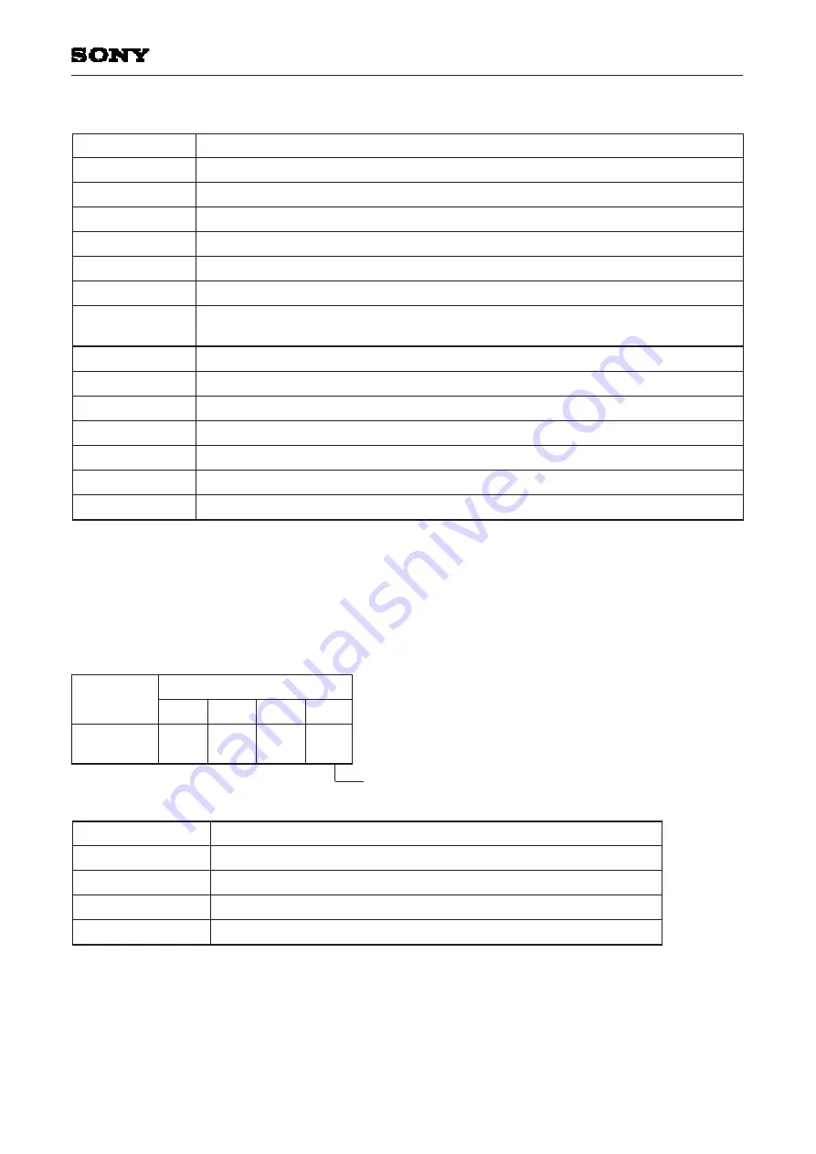
Command bit
EDC7 = 0 EDC6
EDC5
EDC4
EDC3
EDC2
EDC1
EDC0
EDC7 = 1 EDC6
EDC5
EDC4
EDC3
EDC2
EDC1
EDC0
The [No C1 errors, pointer reset] count is output when 0.
The [One C1 error corrected, pointer reset] count is output when 0.
The [No C1 errors, pointer set] count is output when 0.
The [One C1 error corrected, pointer set] count is output when 0.
The [Two C1 errors corrected, pointer set] count is output when 0.
The [C1 correction impossible, pointer set] count is output when 0.
7350 frame count cycle mode
∗
1
when 1.
73500 frame count cycle mode
∗
2
when 0.
The [No C2 errors, pointer reset] count is output when 0.
The [One C2 error corrected, pointer reset] count is output when 0.
The [Two C2 errors corrected, pointer reset] count is output when 0.
The [Three C2 errors corrected, pointer reset] count is output when 0.
The [Four C2 errors corrected, pointer reset] count is output when 0.
The [C2 correction impossible, pointer copy] count is output when 0.
The [C2 correction impossible, pointer set] count is output when 0.
Processing
Error monitor commands
∗
1
The number selected by C1 (EDC1 to 6) and C2 (EDC0 to 6) is added to C1 and C2 and output every 7350
frames.
∗
2
The number selected by C1 (EDC1 to 6) and C2 (EDC0 to 6) is added to C1 and C2 and output every
73500 frames.
$DX commands
See "$CX commands".
Command bit
TB = 0
TB = 1
TP = 0
TP = 1
Bottom hold at a cycle of RFCK/32 in CLVS mode.
Bottom hold at a cycle of RFCK/16 in CLVS mode.
Peak hold at a cycle of RFCK/4 in CLVS mode.
Peak hold at a cycle of RFCK/2 in CLVS mode.
Description
Command
Data 1
CLV CTRL
0
TB
TP
Gain
CLVS
D3
D2
D1
D0
Summary of Contents for PV420S
Page 1: ...SERVICE MANUAL PV420S WWW BBK RU ...
Page 72: ... 69 CXD3068Q Block Diagram ...
Page 73: ... 70 CXD3068Q Pin Configuration ...
Page 122: ... 119 CXD3068Q Timing Chart 1 3 ...
Page 123: ... 120 CXD3068Q Timing Chart 1 4 ...
Page 124: ... 121 CXD3068Q Timing Chart 1 5 ...
Page 129: ... 126 CXD3068Q Timing Chart 2 1 ...
Page 130: ... 127 CXD3068Q Block Diagram 2 2 ...
Page 131: ... 128 CXD3068Q Timing Chart 2 3 ...
Page 134: ... 131 CXD3068Q Timing Chart 2 6 ...
Page 138: ... 135 CXD3068Q VCO C Mode Fig 3 3 Access Flow Chart Using VCO Control ...
Page 140: ... 137 CXD3068Q Block Diagram 4 1 ...
Page 143: ... 140 CXD3068Q Timing Chart 4 4 ...
Page 147: ... 144 CXD3068Q Fig 4 6 a Auto Focus Flow Chart Fig 4 6 b Auto Focus Timing Chart ...
Page 148: ... 145 CXD3068Q Fig 4 7 a 1 Track Jump Flow Chart Fig 4 7 b 1 Track Jump Timing Chart ...
Page 149: ... 146 CXD3068Q Fig 4 8 a 10 Track Jump Flow Chart Fig 4 8 b 10 Track Jump Timing Chart ...
Page 150: ... 147 CXD3068Q Fig 4 9 a 2N Track Jump Flow Chart Fig 4 9 b 2N Track Jump Timing Chart ...
Page 151: ... 148 CXD3068Q Fig 4 10 a Fine Search Flow Chart Fig 4 10 b Fine Search Timing Chart ...
Page 152: ... 149 CXD3068Q Fig 4 11 a M Track Move Flow Chart Fig 4 11 b M Track Move Timing Chart ...
Page 157: ... 154 CXD3068Q Fig 4 15 CD TEXT Data Timing Chart ...
Page 162: ... 159 CXD3068Q Fig 5 3a Fig 5 3b ...
Page 196: ... 193 CXD3068Q Description of Data Readout ...
Page 200: ... 197 CXD3068Q ...
Page 201: ... 198 CXD3068Q ...
Page 202: ... 199 CXD3068Q ...
Page 207: ... 204 CXD3068Q Package Outline Unit mm ...
Page 208: ...This data sheet has been made from recycled paper to help protect the environment 205 ...


