ADM-XRC-5T2-ADV User Manual
ADM-XRC-5T2-ADV User Manual
4.8.
Pn4 I/O
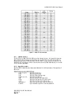
Up to 16 pairs of differential or 32 single-ended signals are available on Pn4 and are sourced
from Bank 18 of the User FPGA. All of the signal traces are routed as 100 Ohm differential
pairs and each pair is matched in length. The worst case difference in trace length between
any two pairs is 10mm. The pairs are distinguished by the signals names listed below and
follow the p/-: 1/3, 2/4, 5/7, 6/8…
Signal
FPGA Pin
Pn4 Pin
Pn4 Pin
FPGA Pin
Signal
PN4_P1
AF11
1 2 AE9
PN4_P2
PN4_N1
AF12
3 4 AE10
PN4_N2
PN4_P3
AF9
5 6 AD8
PN4_P4
PN4_N3
AF10
7 8 AE8
PN4_N4
PN4_P5
AF7 9
10
[CC]
AF5 PN4_P6
PN4_N5 AE7 11
12
[CC]
AF6 PN4_N6
PN4_P7
AC5 [CC]
13
14 [CC]
AB7
PN4_P8
PN4_N7
AC6 [CC]
15
16 [CC]
AB6
PN4_N8
PN4_P9
AG4
[CC]
17 18 AD10
PN4_P10
PN4_N9
AH4
[CC]
19 20 AD11
PN4_N10
PN4_P11
AH6
21 22 AC8
PN4_P12
PN4_N11
AH5
23 24 AC9
PN4_N12
PN4_P13
AB9
25 26 AL5
PN4_P14
PN4_N13
AB8
27 28 AK5
PN4_N14
PN4_P15
AB11
29 30 AJ7
PN4_P16
PN4_N15
AC10
31 32 AK7
PN4_N16
Table 9 Pn4 to FPGA Assignments
In Table 9, pins marked [CC] are clock capable and may be used to access the regional
clocking resources in the FPGA.
Banks 18 is fitted with resistors to allow DCI terminations on Pn4 signals.
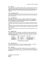
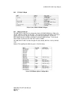
4.8.1. Pn4 Signalling Voltage
The signalling voltage on the Pn4 connector (and User FPGA Bank 18) is selectable by
switch SW2B.
Switch 2B
Pn4 voltage
Open 2.5V
Closed 3.3V
Table 10 Pn4 I/O Voltage Selection
It should be noted that the switch does not directly route power. The switch position is
monitored by the board control logic which, in turn, sets a power multiplexer to be either 2.5V
or 3.3V.
4.9.
XMC Interface
4.9.1. Primary XMC Connector, P15
The MGT (GTP) links connected between the user FPGA and the Primary XMC connector,
P15, are compatible with PCI Express and Serial RapidIO. Depending upon the carrier card,
they may also be used for user-specific applications.
Version 1.0
Page 13


