ADM-XRC-5T2-ADV User Manual
ADM-XRC-5T2-ADV User Manual
4.5.
Clocks
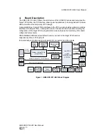
The ADM-XRC-5T2-ADV is provided with numerous clock sources, as shown in Figure 4
below:
Zero-delay
Buffer
(PLL)
Bridge FPGA
(V4LX25)
PCI
Bus
PCI
RefClk
Femto-clock
ICS843034-01
Ctl
25.0 MHz
XTAL
26.5625 MHz
XTAL
User FPGA
Virtex5
LX220T /
LX330T
XTAL_CLK
Local Bus
LCLK
Bridge Config
(Coolrunner)
USERMGT_CLKA
USERMGT_CLKB
PCIe_RefClk (100 MHz)
200 MHz
Osc.
REFCLK_200M
PCI-X
CLK
PCI
CLK
FCN_MGTREF
Pn4 Connector
KEY
Global Clock Inputs
Clock Capable I/O
MGT Clock Inputs
156.25 MHz
Osc.
Figure 4 Clock Structure
4.5.1. LCLK
The Local Bus can be used at up to 80 MHz and all timing is synchronised to LCLK between
the Bridge and User FPGAs. LCLK is generated from a 200MHz reference by a DCM within
the bridge FPGA. The minimum LCLK frequency (determined by the DCM specification) is
32MHz.
The LCLK frequency is set by writing to the board control logic. (See SDK for details and
example application).
Note: If the user FPGA application includes a DCM driven by LCLK (or one of the other
programmable clocks), the clock frequency should be set prior to FPGA configuration.
Version 1.0
Page 7


