background image


ADM-XRC-5T2-ADV User Manual 


ADM-XRC-5T2-ADV User Manual 

4.6.2.  I/O Bank Voltages 


Bank Voltage 

Description 

0 3.3V 

Configuration 

I/F 

1, 4, 5, 6 

1.5V 

DDRII SRAM 

3.3V 

SelectMAP I/F, Serial Flash 

3 3.3V 

Clocks 

19, 21, 23, 25 

1.8V 

DDRII DRAM 

27, 29, 31, 33 

1.8V 

DDRII DRAM (LX330T only) 

18 

2.5V or 3.3V 

Pn4 Interface 

11, 13, 15, 17, 26 

3.3V 

ADV212 Interface 

12, 20, 24 

1.8V 

Local Bus 

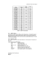
Table 4  User FPGA I/O Bank Voltages 

4.6.3.  Memory Interfaces 

The ADM-XRC-5T2-ADV has four independent banks of DDRII SDRAM when fitted with a 
LX330T, SX240T or FX200T target FPGA.  (Two banks with all smaller FPGAs)  Each bank 
consists of two memory devices in parallel to provide a 32 bit datapath.  1Gb Micron 
MT47H64M16 devices are fitted as standard to provide 256MB per bank.  The board will 
support higher capacity devices when they become available. 

The ADM-XRC-5T2-ADV has been designed for compatibility with Xilinx memory interface 
cores. 

Details of the signalling standards are given in the table below: 


Name Direction 

I/O 

Standard 

DDR_ad[15:0], 
DDR_ba[2:0], 
DDR_rasn, 
DDR_casn, 
DDR_wen, 
DDR_csn, 
DDR_cke, 
DDR_odt 

Output SSTL18_I_DCI 

DDR_ck0, 
DDR_ckn0 

Output DIFF_SSTL18_II 

DDR_dq[15:0] BiDir 

SSTL18_II 

DDR_dm[1:0] Output 

SSTL18_II_DCI 

DDR_dqs[1:0], 
DDR_dqsn[1:0] 

BiDir DIFF_SSTL18_II 

DDR_ck1, 
DDR_ckn1 

Output DIFF_SSTL18_II 

DDR_dq[31:16] BiDir 

SSTL18_II 

DDR_dm[3:2] Output 

SSTL18_II_DCI 

DDR_dqs[3:2], 
DDR_dqsn[3:2] 

BiDir DIFF_SSTL18_II 

Table 5  DDR Memory Bank Configuration 

Version 1.0 

Page 10


Summary of Contents for ADM-XRC-5T2-ADV

Page 1: ...ADM XRC 5T2 ADV PCI Mezzanine Card JPEG2000 Video Compression Multi Gigabit Serial I O User Guide Version 1 0...

Page 2: ...ta 4 West Silvermills Lane Edinburgh EH3 5BD UK Phone 44 0 131 558 2600 Fax 44 0 131 558 2700 Email support alphadata co uk Alpha Data 2570 North First Street Suite 440 San Jose CA 95131 USA Phone 408...

Page 3: ...ks 7 4 5 1 LCLK 7 4 5 2 REFCLK 8 4 5 3 PCIe Reference Clock 8 4 5 4 User MGT Clocks 8 4 5 5 FCN MGT Clock 8 4 5 6 Rear Pn4 Clocks 8 4 5 7 PCI Clocks 8 4 6 User FPGA 9 4 6 1 Configuration 9 4 6 2 I O B...

Page 4: ...A I O Bank Voltages 10 Table 5 DDR Memory Bank Configuration 10 Table 6 FCN Interface MGT Links 11 Table 7 Board Control Signals 12 Table 8 Optical Module Control Signals 12 Table 9 Pn4 to FPGA Assign...

Page 5: ...to integrate proprietary cores into the FPGA Physically conformant to VITA 42 XMC Standard Physically conformant to IEEE P1386 2001 Common Mezzanine Card standard with XMC connector removed 8 lane PCI...

Page 6: ...fitted to an ADC PMC carrier board The ADC PMC can support up to two PMC cards whilst maintaining host PC PCI compatibility If you are using a ADC PMC refer to the supplied documentation for informat...

Page 7: ...ard voltage and temperature DDR2 SDRAM SSRAM and serial flash memory connect to the target FPGA and are supported by Xilinx or third party IP IO functionality is provided using multi gigabit I O conne...

Page 8: ...bidir Address and data bus lbe_l 7 0 bidir Byte qualifiers lads_l bidir Indicates address phase lblast_l bidir Indicates last word lbterm_l bidir Indicates ready and requests new address phase lready_...

Page 9: ...sh An ST M25P32 flash memory with SPI interface is connected to the User FPGA for the storage of application specific information 4 3 Health Monitoring The ADM XRC 5T2 ADV has the ability to monitor t...

Page 10: ...e FPGA using the Xilinx tools and serial download cables This also allows the use of ChipScope PRO ILA to debug an FPGA design It should be noted that four devices will be detected when the SCAN chain...

Page 11: ...r KEY Global Clock Inputs Clock Capable I O MGT Clock Inputs 156 25 MHz Osc Figure 4 Clock Structure 4 5 1 LCLK The Local Bus can be used at up to 80 MHz and all timing is synchronised to LCLK between...

Page 12: ...B is connected to an MGT clock input on the bottom half of the user FPGA It may be used as the reference for the front user MGTs See Table 3 for details of the MGT clock connections Note Either of the...

Page 13: ...The ADM XRC 5T2 ADV performs configuration from the host at high speed using SelectMAP The FPGA may also be configured from flash or by JTAG via header J2 Download from the host is the fastest way to...

Page 14: ...arallel to provide a 32 bit datapath 1Gb Micron MT47H64M16 devices are fitted as standard to provide 256MB per bank The board will support higher capacity devices when they become available The ADM XR...

Page 15: ...D2 120A S14 FCN_TX5_N E2 S13 FCN_RX5_P E1 S3 FCN_RX5_N F1 S4 FCN_TX6_P B1 124B S12 FCN_TX6_N B2 S11 FCN_RX6_P A2 S5 FCN_RX6_N A3 S6 FCN_TX7_P B6 124A S10 FCN_TX7_N B5 S9 FCN_RX7_P A5 S7 FCN_RX7_N A4...

Page 16: ...5Gb s over copper or optical fibre Dual 10Gb s Ethernet CX4 4 lanes at 3 125Gb s over copper or optical fibre Dual 10Gb s FibreChannel 4 lanes at 3 1875Gb s over copper or optical fibre Dual 4 x OC 4...

Page 17: ...N11 AH5 23 24 AC9 PN4_N12 PN4_P13 AB9 25 26 AL5 PN4_P14 PN4_N13 AB8 27 28 AK5 PN4_N14 PN4_P15 AB11 29 30 AJ7 PN4_P16 PN4_N15 AC10 31 32 AK7 PN4_N16 Table 9 Pn4 to FPGA Assignments In Table 9 pins mark...

Page 18: ...ADV212 Interface The ADV212 is a single chip JPEG 2000 codec from Analog Devices It is targeted for video and high bandwidth image compression applications that can benefit from the enhanced quality a...

Page 19: ...mclk T37 AJ42 vclk Y42 AK8 field F41 AT5 hsync E40 AG12 vsync F40 AG9 jpeg_reset_l L42 AN41 scomm5 AF42 AF37 adv_hdata 0 AA39 AR40 adv_hdata 1 AA41 AT40 adv_hdata 2 AA40 AB34 adv_hdata 3 AA37 AP40 adv...

Page 20: ...8 H41 W41 AM9 AH9 vdat 9 G41 U41 AG8 AH10 vdat 10 F42 U39 AH8 AJ10 vdat 11 G42 V41 AP8 AG11 dack_l 0 H38 T40 AM37 AK42 dack_l 1 F39 U42 AE37 AJ40 dreq_l 0 E39 T42 AN38 AK39 dreq_l 1 G38 T39 AL37 AT41...

Page 21: ...ADM XRC 5T2 ADV User Manual ADM XRC 5T2 ADV User Manual Version 1 0 Page 17 5 1 Revision History Date Revision Nature of Change 16 Dec 2008 1 0 Initial version...

Reviews: