background image

Yok

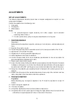
Fig. 1 

2.1.4 Turn both tabs at the same time keeping the angle constant to superimpose red and blue

horizontal on the center of the screen. 

2.1.5 Adjust two tabs of the 6-pole magnet to superimpose red/blue line and green line. 
2.1.6 Remember red and blue movement. Repeat steps 2.1.3 2.1.5 until optimal convergence is

obtained.

2.2 Circumference convergence adjustment 
2.2.1

Loosen the clamp screw holding the deflection yoke assembly and allow it tilting. 

2.2.2

Temporarily put the first wedge between the picture tube and deflection yoke assembly.
Move front of the deflection yoke up or down to obtain better convergence in circumference.
Push the mounted wedge in to fix the yoke temporarily. 

2.2.3

Put the second wedge into bottom. 

2.2.4

Move  front  of  the  deflection  yoke  to  the  left  or  right  to  obtain  better convergence  in
circumference.

2.2.5

Fix the deflection yoke position and put the third wedge in either upper space. Fasten the
deflection yoke assembly on the picture tube. 

2.2.6

Detach  the  temporarily  mounted wedge  and put  it  in  either  upper space.  Fasten  the
deflection yoke assembly on the picture tube. 

2.2.7

After fastening the three wedges, recheck overall convergence and ensure to get optimal 
convergence. Tighten the lamp screw holding the deflection yoke assembly. 

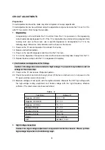
3. White Balance Adjustment 

Generally, white balance adjustment is made with professional equipment. It’s not practical to
get good white balance only through manual adjustment. For TVs with I

2

C bus control, change

the bus data to adjust white balance. 

6

Summary of Contents for 25CT23FSR

Page 1: ...SERVICE MANUAL Models 25CT23FSR 29CT23FSR www akai ru COLOUR TV SET ...

Page 2: ...L DESCRIPTION 3 MAINTENANCE 4 ADJUSTMENTS 5 SET UP ADJUSTMENTS 5 CIRCUIT ADJUSTMENTS 8 STRUCTURE AND CHASSIS FUNCTION DESCRIPTION 14 STRUCTURE BLOCK DIAGRAM 14 BLOCK DIAGRAM FOR SUPPLY VOLTAGE SYSTEM 15 CHASSIS DESCRIPTION 16 SERVICE DATA 17 TECHNICAL DATA OF KEY ICS 17 WAVEFORMS OF KEY POINTS 35 SERVICE DATA OF KEY ICS 38 REPLACEMENT OF PARTS 44 APPENDIX 1 CIRCUIT DIAGRAM 1 ...

Page 3: ...um EHT voltage does not exceed the rated value after service and adjustment SAFETY PRECAUTION WARNING REFER SERVICING TO QUALIFIED SERVICE PERSONNEL ONLY 1 The TV has a nominal working EHT voltage Extreme caution should be exercised when working on the TV with the back removed 1 1 Do not attempt to service this TV if you are not conversant with the precautions and procedures for working on high vo...

Page 4: ...s read the parts list in this manual carefully Substitute replacement components which do not have the same safety characteristics as specified in the parts list may create X ray radiation 2 Do not slap or beat the cabinet or CRT since this may result in fire or explosion 3 Never allow the TV sharing a plug or socket with other large power equipment Doing so may result in too large load causing fi...

Page 5: ...gister or where it is exposed to direct sunlight 2 Do not install the TV set in a place exposed to rain water excessive dust mechanical vibrations or impacts 3 Allow enough space at least 10cm between the TV and wall or enclosures for proper ventilation 4 Slots and openings in the cabinet should never be blocked by clothes or other objects 5 Please power off the TV set and disconnect it from the w...

Page 6: ...s to the end and rotate the green low brightness potentiometer to center 1 7 Receive green raster pattern signals 1 8 Loosen the clamp screw holding the deflection yoke assembly and slide it forward or backward to display a vertical green zone on the screen Rotate and spread the tabs of the purity magnet around the neck of the CRT until the green zone is located vertically at the center of the scr...

Page 7: ...in to fix the yoke temporarily 2 2 3 Put the second wedge into bottom 2 2 4 Move front of the deflection yoke to the left or right to obtain better convergence in circumference 2 2 5 Fix the deflection yoke position and put the third wedge in either upper space Fasten the deflection yoke assembly on the picture tube 2 2 6 Detach the temporarily mounted wedge and put it in either upper space Fasten...

Page 8: ...Center Convergence by Convergence Magnets Incline the Yoke Up or Down Incline the Yoke Right or Left Fig 2 4 pole Magnet Movement 6 pole Magnet Movement Circumference Convergence by DEF Yoke Fig 3 7 ...

Page 9: ...nd slowly take it away from the TV 1 5 Repeat the above steps until the TV is degaussed completely 2 Confirmation and Adjustment for Voltage Caution B voltage has close relation to high voltage To prevent X ray radiation set B voltage to the rated value 2 1 Power on the TV and receive Philips test pattern 2 2 Check the resistors and coils for being burned If the fuse is burned out do not power on ...

Page 10: ... 3 Receive a normal TV signal Rotate knob of the FCB until you get a sharp picture Before Adjusting After Adjusting Fig 4 5 Safety Inspection 5 1 Inspection for insulation and voltage resistant Perform safety test for all naked metal of the TV Supply high voltage of 3000V 50Hz limit current of 10mA between all naked metal and cold ground Test every point for 3 sec and ensure no arcing and sparking...

Page 11: ...tput VA Set to the optimum Vertical amplitude When vertical frequency is identified to 50Hz 5VA is displayed when identified to 60Hz 6VA displayed SC Set to the optimum S correction VSH Set to the optimum Vertical shift When vertical frequency is identified to 50Hz 5VSH is displayed when identified to 60Hz 6VSH displayed 5OV Set to the optimum Character field starting position When vertical freque...

Page 12: ...e YDFP 0D Brightness delay PAL YDFN 0D Brightness delay NTSC YDFS 0D Brightness delay SECAM YDAV 0D AV brightness delay AGC Set to the optimum Automatic gain control AGC VOL 28 Volume initial value IFFS O3 Intermediate frequency CL OB AGCS 03 AGC speed VG2B 30 VG2 brightness SVOL 36 Volume 00 MVOL 3C Volume 25 SBRI 1F Sub brightness MBRI 33 Brightness Max SCON 0C Sub contrast MCON 3F Contrast Max ...

Page 13: ...German 6 OP_ITALY Italian OP3 7 OP_SPAIN Spanish 0 OP_FMWS Window selection of sound PLL 1 Large window 0 Small window 1 OP_DIRECT_SWITCH_ ON Memory on 1 Remote on if remote off instant on if AC off 0 Soft on 2 OP_HCO EHT EW control 1 On 0 Off 3 OP_CHH_LOGO Changhong logo display 1 Yes under no signal condition 0 No 4 OP_SOUND_DK Audio system DK option 1 Yes 0 No 5 OP_SOUND_BG Audio system BG opti...

Page 14: ...PSNS Sensitivity 2 OP_BSCREEN Black screen when changing channels 1 Yes 0 No 3 OP_SECAM SECAM option 1 Yes 0 No 4 OP_DFL Disable flash protection 5 OP_SIF SIF selection 1 External 0 Internal 6 OP_EXT_SIF0 OP6 7 OP_EXT_SIF1 External circuit sound system selection SIF1 SIF0 00 DK 01 BG 10 I 11 M Activated with OP SIF Table 5 TAB data check sheet O P1 O P2 O P3 O P4 O P5 O P6 VX00 YD FP FN FS AV AG C...

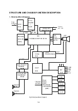
Page 15: ... OUT V436 CRT Drive TDA6107Q NY01 Audio Amplifier TDA7057AQ N600 Analog switch HEF4053 N350 Audio Processor TDA9859 N606 SDA SCL CRT Band 1 2 Vt AGC I2 C BUS FBT T400 V OUT R AMP Speaker R Speaker L Power Supply Circuit STR F6454R or STR F6656 N801 145V 16V S 5V 2 3 2V 150 250V AC 50Hz V OUT TDA8350 N400 15V YUV In AV I O 190V 45V 16V 8V 5V 1 Fig 5 Structure Block Diagram 14 ...

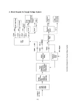
Page 16: ...2 Block Diagram for Supply Voltage System Fig 6 Block Diagram for Supply Voltage System 150 250V AC 50Hz 15 ...

Page 17: ...ing features are available in the chassis PAL NTSC SECAM reception Real time clock Child lock Alarm Electronic program guide Auto identification of video signal source Auto identification of color audio system AV input output CCD V CHIP PAL NTSC D COMB HI FI stereo Surround The chassis mainly uses the following ICs and assemblies Table 6 Key ICs and Assemblies Serial No Position Type Function Desc...

Page 18: ...M sound frequencies 4 5 5 5 6 0 6 5 MHz The quality of this system is such that the external band pass filters can be omitted Source selection between internal CVBS and external CVBS or Y C signals Integrated chrominance trap circuit Integrated luminance delay line with adjustable delay time Picture improvement features with peaking with variable centre frequency and positive negative overshoot ra...

Page 19: ...6 bit output Data Capture Text memory for 0 1 or 10 pages In the 10 page versions inventory of transmitted Teletext pages stored in the Transmitted Page Table TPT and Subtitle Page Table SPT Data Capture for US Closed Caption Data Capture for 525 625 line WST VPS PDC system A and Wide Screen Signalling WSS bit decoding Automatic selection between 525 WST 625 WST Automatic selection between 625 WST...

Page 20: ... 4 5 6 5 MHz with switchable centre frequency Audio switch Automatic Volume Levelling Automatic Volume Levelling or subcarrier output for combfilter applications Qss sound IF amplifier with separate input and AGC circuit AM sound demodulator without extra reference circuit PAL decoder SECAM decoder NTSC decoder Horizontal geometry E W Horizontal and Vertical Zoom ROM size User RAM size Teletext Cl...

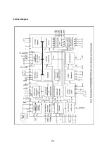
Page 21: ... 3 Block Diagram 7 20 ...

Page 22: ...8 21 ...

Page 23: ... 4 Pining 5 Refer to Table 12 about Functions and Data of the IC s Pins 9 22 ...

Page 24: ...0 and Y1 and the other side connected to a common input output Z With E cted lo LOW one of the two switches is sele w impedance ON state by Sn With E HIGH all switches are in the high impedance OFF state independent of SA to SC VDD and VSS are the supply voltage connections for the digital control inputs SA to SC and E The VDD to VSS range is 3 to 15V The analog inputs outputs Y0 Y1 and Z can swin...

Page 25: ...ltage drop across the switch but the voltages at Y and Z may not exceed VDD or VEE Refer to Table 13 about Functions and Data of the IC s Pins H H 4 HEF4053T D 16 lead S0 plastic SOT109 1 Package Designator North America R L S N 4 Fig 11 Pinning Diagram EF4053P N 16 lead DIL plastic SOT38 1 EF4053D F 16 lead DIL ceramic cerdip SOT7 Y1A to Y1C Independent inputs outputs SA to Sc Select inputs E Ena...

Page 26: ...he device is designed for use in TVs and monitors but is also suitable for battery fed portable recorders and radios Missing Current Limiter MCL A MCL protection circuit is built in The MCL circuit is activated when the difference in current between the output terminal of each amplifier exceeds 100 mA typical 300 mA This level of 100 mA allows for single ended headphone applications 3 Block Diagra...

Page 27: ...TDA8356 is a power circuit for use in 9 colour deflection systems for field frequencies of 50 to 120 Hz The circuit provides a DC driven vertical deflection output circuit efficient class G system Block Diagram eatures ighly efficient fully DC coup t bridge circuit Vertical flyback Guard circuit Protection against Short circuit of the output pins 7 and emperature protection e inputs 0 and 110 Gene...

Page 28: ...drive neg 2 Input power stage negative includes II sb signal bias VP 3 Operating supply voltage VO B 4 Output voltage B GND 5 Ground VFB 6 Input flyback supply voltage VO A 7 Output voltage A VO guard 8 Guard output voltage VI fb 9 Input feedback voltage 5 Refer to Table 15 about Functions and Data of the IC s Pins 27 ...

Page 29: ...and pseudo stereo effects Audio surround decoder can be added externally Two general purpose logic output ports I2 C bus control of all functions 2 General Description The TDA9859 provides control facilities for the main and the SCART channel of a TV set Due to extended switching possibilities signals from three stereo sources can be handled 3 Block Diagram 4 Refer to Table 16 about Functions and ...

Page 30: ...olded SIP style package affording dielectric isolation without compromising thermal characteristics 1 Features Flyback Operation with Quasi Resonant Soft Switching for Low Power Dissipation and EMI Rugged Avalanche Rated MOSFET Soft drive circuit MOSFET Adjustable MOSFET switching speed Choice of MOSFET Voltage and rDS on Full Over Current Protection no blanking Under Voltage Lockout with Hysteres...

Page 31: ... 2 Circuit Block Diagram Dwg MK 003 50mm Fig 18 Fig 17 3 Pin Configuration and Functions 30 ...

Page 32: ...r STR F6454R F6656 Symbol Function Description 1 OCP FB Over current protection detection signal voltage limiting signal input 2 S MOSFET source 3 D MOSFET drain 4 VIN Supply voltage input for control circuit 5 GND Ground 31 ...

Page 33: ...2 General Description The TDA6107Q 6108JF includes three video ent SIL 9 pin medium power DBS9MPF package SOT 111 1 using high voltage DMOS technology nded to drive the three cathodes of a colour CRT directly To obtain maximum performance the amplifier should be used with black current control 3 Ordering Information Table 10 Package F or 5 5MHz for TDA6107Q output amplifiers in one plastic DIL b 6...

Page 34: ...ing input 2 Vi 3 3 Inverting input 3 GND 4 ground fin Iom 5 Black current measurement output VDD 6 Supply voltage Voc 3 7 Cathode output 3 Voc 2 8 Cathode output 2 Voc 1 20 Pin Co 5 Refer to Table 17 about Functions and Data of the IC s Pins Fig nfiguration 9 Cathode output 1 33 ...

Page 35: ...puts for noise suppression with Schmitt trigger Clock frequency up to 400 kHz High programming flexibility Internal programming voltage Self timed programming cycle including erase Byte write and page write programming between 1 and 16 bytes Typical programming time 6 ms 10 ms for up to 16 bytes Endurance 106 cycles1 Data retention 40 years1 ESD protection 4000 V on all pins 8 pin DIP DSO packages...

Page 36: ...35 y Points IN7 4 TDA938X 5 TDA938X PIN22 6 TDA938X PIN26 2 Waveforms of Ke 1 TDA938X PIN4 2 TDA938X PIN5 3 TDA938X P PIN8 ...

Page 37: ...7 TDA938X PIN31 8 TDA938X PIN33 TDA938X PIN34 10 TDA938X PIN38 11 TDA938X PIN40 12 TDA938X PIN42 9 36 ...

Page 38: ...13 TDA938X PIN44 14 TDA938X PIN49 Flyback Pulse 17 Waveform of Line Drive Voltage 18 Waveform of Horizontal Scan Current 19 Waveform of Vertical Scan Current 15 TDA938X PIN58 16 Horizontal 37 ...

Page 39: ... 1 6 1 63 6 P3 1 ADC1 PWM1 0 1 4 87 4 87 7 P3 2 ADC2 PWM2 0 02 7 55 7 57 8 P3 3 ADC3 PWM3 0 02 7 54 7 55 9 0 P C S S V 0 0 10 2 0 0 5 0 P 4 88 4 9 11 6 0 3 6 0 P 5 05 5 07 12 0 A S S V 0 0 13 9 2 2 L L P C E S 21 46 27 35 14 6 8 7 2 P V 1 27 1 29 15 9 9 4 G I D C E D 16 2 23 33 16 PH2LF 3 43 21 01 27 32 17 PH1LF 3 9 21 33 27 58 18 0 3 D N G 0 0 19 9 9 3 G B C E D 18 75 24 58 20 AVL EW 20 36 26 37 ...

Page 40: ...AUDEXT 1 98 8 48 8 66 37 QSSO AMOUT 1 2 44 21 48 1 98 38 AUDEXT 2 87 21 62 23 98 39 QSSO AMOUT 1 7 86 1 26 1 31 40 AUDEXT 6 6 3 21 24 27 2 41 GND1 0 0 0 42 CVBS Y 3 76 21 12 27 2 43 CHROMA 1 83 1 26 67 48 44 AUDOUT AMOUT 1 3 56 21 97 27 71 45 INSSW 8 6 1 2 19 35 22 46 46 R2 VIN 2 54 21 7 1 83 47 G2 YIN 2 54 21 76 1 83 48 B2 UIN 2 54 21 76 1 83 49 BCLIN 2 21 76 27 1 71 50 BLKIN 3 19 20 81 21 25 51 ...

Page 41: ...t 2 5 0 0 5 Table 13 Functions and Service Data of HEF4053 N350 s Pins Digital Multime Victor DT890D Pin No ription Reference Voltage Positive Resistance Negative Resistance Signal input 2 4 6 0 d n u o r G 0 0 7 0 d n u o r G 0 0 8 0 d n u o r G 0 0 9 Control signal input 0 03 13 5 13 1 10 Control signal input 0 03 13 5 13 1 11 Control signal input 0 03 13 5 13 1 12 Signal input 3 9 22 2 47 0 13 ...

Page 42: ...annel in phase signal t 7 35 18 74 21 49 0 0 0 7 18 4 21 47 ght channe tput 2 0 0 ight channe tput Voltag K K 1 Idr 4 ive pos 2 27 7 20 3 2 Idr 4 ive neg 2 27 7 20 4 P 5 GND 0 0 0 6 V 0 3 FB 45 113 13 7 7 V 5 1 O A 7 6 6 1 9 0 d n u o r G 1 Left channel inverting signal output 39 7 11 Ri l inverting signal ou 7 39 18 47 21 47 1 0 d n u o r G 13 R l in phase signal ou 7 4 16 47 21 46 Table 15 Funct...

Page 43: ...19 8 Ground 0 0 0 9 Audio output 3 85 19 93 26 27 10 Audio input 8 3 85 19 93 26 31 11 Channel 1 audio ation 3 85 20 67 25 854 compens 12 Channel 2 audio compensation 3 85 21 45 27 59 4 ge for filtering 7 63 7 39 13 Audio output 8 0 01 14 Treble compensation 3 84 22 31 27 01 15 2 9 58 6 64 7 Serial data line 8 54 62 9 Treble compensati 0 Audio output 1 Bass2 compensation 5 44 7 55 3 Audio input 5 ...

Page 44: ...200 s Pins Digital Multimeter ice 08 N Function V 20K 20K 2 Address input 0 0 0 3 Address input 4 93 3 18 3 2 4 Common ground 0 0 0 6 Data line 3 42 6 56 6 64 7 PW write protect 0 20 78 Pin No Function Description Reference Voltage V Positive Resistance 20K Negative Resistance 20K 1 G inverting input 3 33 5 32 4 72 2 R inverting input 3 26 5 32 4 72 3 B inverting input 3 28 5 32 4 72 5 Black level...

Page 45: ...entified by the A marking have special safety related characteristics A pecial safety related characteristics CB The components identified by the CB marking have been evaluated to the CB standard The components identified by li G The components identified by the G m ing have critic cteristics Z The components identified by the Z marking have important characteristics De ription characteristics his...

Page 46: ...CIRCUIT DIAGRAM JUC 820 975 JUC 820 591 JUC 820 725 JUC 820 644 APPENDIX ...

Reviews: