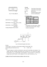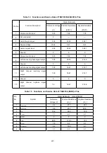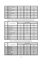
Table 11 Pinning
Symbol Pin Description
V
i(1)
1
Inverting input 1
V
i(2)
2
Inverting input 2
V
i(3)
3
Inverting input 3
GND
4
ground (fin)
I
om
5
Black-current
measurement output
V
DD
6
Supply voltage
V
oc(3)
7
Cathode output 3
V
oc(2)
8
Cathode output 2
V
oc(1)
. 20 Pin Co
(5) Refer to Table 17 about Functions and Data of the IC’s Pins.
Fig
nfiguration.
9
Cathode output 1
33
Summary of Contents for 25CT23FSR
Page 1: ...SERVICE MANUAL Models 25CT23FSR 29CT23FSR www akai ru COLOUR TV SET ...
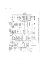
Page 21: ... 3 Block Diagram 7 20 ...
Page 22: ...8 21 ...
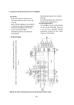
Page 23: ... 4 Pining 5 Refer to Table 12 about Functions and Data of the IC s Pins 9 22 ...
Page 31: ... 2 Circuit Block Diagram Dwg MK 003 50mm Fig 18 Fig 17 3 Pin Configuration and Functions 30 ...
Page 46: ...CIRCUIT DIAGRAM JUC 820 975 JUC 820 591 JUC 820 725 JUC 820 644 APPENDIX ...


