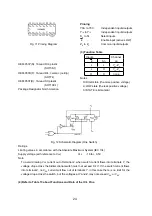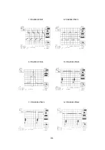
Pinning
Fig. 12 Schematic Diagram (One Switch)
atings
imiting values in accordance with the Absolute Maximum System (IEC 134)
upply voltage (with reference to V
DD
) V
EE
-18 to + 0,5V
ote
To avoid drawing V
DD
current out of terminal Z, when switch current flows into terminals Y, the
voltage drop across the bidirecctional switch must not exceed 0,4 V. If the switch current flows
into terminal Z, no V
DD
current will flow out of terminals Y, in this case there is no limit for the
voltage drop across the switch, but the voltages at Y and Z may not exceed V
DD
or V
EE
.
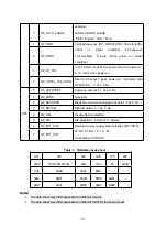
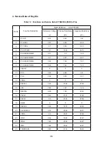
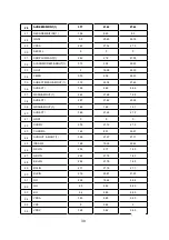
) Refer to Table 13 about Functions and Data of the IC’s Pins.
H
H
4)
HEF4053T(D): 16-lead S0; plastic
(SOT109-1)
Package Designator North America
R
L
S
N
(4
Fig. 11 Pinning Diagram
EF4053P(N): 16-lead DIL; plastic
(SOT38-1)
EF4053D(F): 16-lead DIL; ceramic (cerdip)
(SOT7
Y
1A
to Y
1C
Independent inputs/outputs
S
A
to Sc
Select inputs
E
Enable input (active LOW)
Z
A
to Z
C
Common inputs/outputs
(3) Function Table
Inputs
E
Sn
Channel
on
L
L
Y
0n
-Z
n
L
H
Y
1n
-Z
n
H
X
none
Notes
H=HIGH state (the more positive voltage)
L=LOW state (the less positive voltage)
al
X=STATE is immateri
Y0A to Y0C Independent inputs/outputs
24
Summary of Contents for 25CT23FSR
Page 1: ...SERVICE MANUAL Models 25CT23FSR 29CT23FSR www akai ru COLOUR TV SET ...
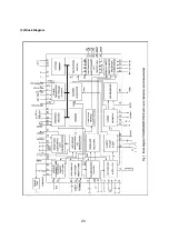
Page 21: ... 3 Block Diagram 7 20 ...
Page 22: ...8 21 ...
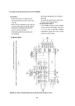
Page 23: ... 4 Pining 5 Refer to Table 12 about Functions and Data of the IC s Pins 9 22 ...
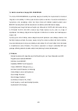
Page 31: ... 2 Circuit Block Diagram Dwg MK 003 50mm Fig 18 Fig 17 3 Pin Configuration and Functions 30 ...
Page 46: ...CIRCUIT DIAGRAM JUC 820 975 JUC 820 591 JUC 820 725 JUC 820 644 APPENDIX ...


