1.7 Triple Video Output Amplifier TDA6108JF/6107Q
(1) Features
Typical bandwidth of 9.0MHz (for
TDA6108J
for an output signal of
k
value)
High ew rate
850
TDA6108JF)
s
(for
TDA6107Q)
No external components required
Very simple application
Single supply voltage of 200 V
Internal reference voltage of 2.5 V
Fixed gain of 51 (for TDA6108JF) or 50 (for
TDA6107Q)
Black-Current Stabilization (BCS) circuit
Thermal protection.
(2) General Description
The TDA6107Q/6108JF includes three video
ent-SIL
9-pin medium power (DBS9MPF) package (SOT
111-1), using high-voltage DMOS technology,
nded to drive the three cathodes of a
colour CRT directly. To obtain maximum
performance, the amplifier should be used with
black-current control.
(3) Ordering Information
Table 10
Package
F) or 5.5MHz (for TDA6107Q)
output amplifiers in one plastic DIL-b
60 V (peak-to-pea
sl
of 1
V/ s (for
and is inte
or
900V/
Type
Number
Name
Description
Version
TDA6108JF/
TDA6107Q
DBS9MPF
Plastic
DIL-bent-SIL
medium power
package with fin;
9 leads
SOT111-1
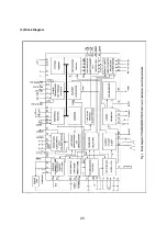
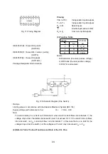
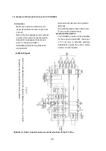
(4) Block Diagram
Fig. 19
32
Summary of Contents for 25CT23FSR
Page 1: ...SERVICE MANUAL Models 25CT23FSR 29CT23FSR www akai ru COLOUR TV SET ...
Page 21: ... 3 Block Diagram 7 20 ...
Page 22: ...8 21 ...
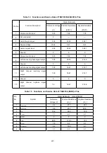
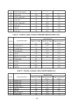
Page 23: ... 4 Pining 5 Refer to Table 12 about Functions and Data of the IC s Pins 9 22 ...
Page 31: ... 2 Circuit Block Diagram Dwg MK 003 50mm Fig 18 Fig 17 3 Pin Configuration and Functions 30 ...
Page 46: ...CIRCUIT DIAGRAM JUC 820 975 JUC 820 591 JUC 820 725 JUC 820 644 APPENDIX ...


