– 35 –
ADJUSTMENT (TUNER / DECK / FRONT / CD)
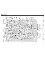
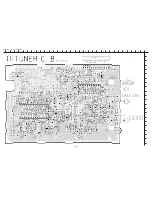
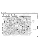
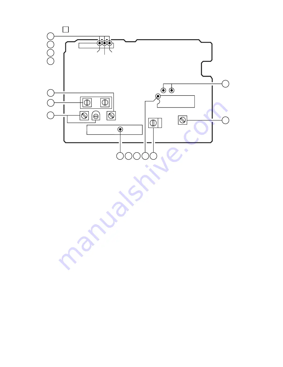
< TUNER SECTION >
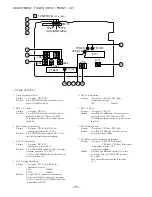
1. Clock Frequency Check
Settings :
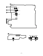
• Test point : TP2 (CLK)
Method :
Set to MW 1602kHz and check that the test
point is 2052kHz
±
45Hz.
2. MW VT Check
Settings :
• Test point : TP1 (VT)
Method :
Set to MW 1602kHz and check that the test
point is less than 8.0V. Then set to MW
531kHz and check that the test point is more
than 0.6V.
3. MW Tracking Adjustment
Settings :
• Test point : TP8 (Lch), TP9 (Rch)
• Adjustment location : L981 (1/3)
Method :
Set to MW 999kHz and adjust L981 (1/3) so
that the test point becomes maximum.
4. LW VT Adjustment
Settings :
• Test point : TP1 (VT)
• Adjustment location : L942
Method :
Set to LW 144kHz and adjust L942 so that the
test point becomes 1.3V
±
0.05V.
Then set to LW 290kHz and check that the test
point is less than 8.0V.
5. LW Tracking Adjustment
Settings :
• Test point : TP8 (Lch), TP9 (Rch)
• Adjustment location :
L941 ........................... 144kHz
TC942 ......................... 290kHz
Method :
Set up TC942 to center before adjustment.
The level at 144kHz is adjusted to maximum
by L941. Then the level at 290kHz is adjusted
to maximum by TC942.
6. AM IF Adjustment
Settings :
• Test point : TP8 (Lch), TP9 (Rch)
• Adjustment location :
L772 ........................... 450kHz
7. FM VT Check
Settings :
• Test point : TP1 (VT)
Method :
Set to FM 108.0MHz and check that the test
point is less than 8.0V. Then set to FM
87.5 MHz and check that the test point is more
than 0.5V.
8. FM Tracking Check
Settings :
• Test point : TP8 (Lch), TP9 (Rch)
Method :
Set to FM 98.0MHz and check that the test
point is less than 13dB
µ
V.
9. DC Balance / Mono Distortion Adjustment
Settings :
• Test point : TP3,TP4 (DC balance)
TP8 (Lch), TP9 (Rch) (Distortion)
• Adjustment location : L771
• Input level : 60dB
µ
V
Method :
Set to FM 98.0MHz and adjust L771 so that
the voltage between TP3 and TP4 becomes
0V
±
0.04V.
Next, check that the distortion is less than
1.3%.
L771
L981
L772
FFE801
1
IC771
TP1(VT)
TP2(CLK)
TP4(DC)
TP3(DC)
1
CN701
(GND)
TP8
(LCH)
TP9
(RCH)
TUNER C.B
C
1
2
3
3
5
6
4
6
8
10
9
9
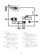
L942
L941
TC942
5
7
4
11
O TUNER C.B
<EZ,K ONLY>
Summary of Contents for XR-MD510
Page 5: ... 5 ...
Page 15: ... 15 SCHEMATIC DIAGRAM 1 MAIN PT1 PT2 RELAY ...
Page 17: ... 17 SCHEMATIC DIAGRAM 2 FRONT SW 1 SW 2 FACE A FACE B FACE C DECK ...
Page 20: ... 20 SCHEMATIC DIAGRAM 3 CD CD LOAD CD DRIVE ...
Page 22: ... 22 SCHEMATIC DIAGRAM 4 D TUNER ...
Page 24: ... 24 SCHEMATIC DIAGRAM 5 K TUNER ...
Page 26: ... 26 SCHEMATIC DIAGRAM 6 EZ TUNER ...
Page 29: ... 29 IC BLOCK DIAGRAM IC BA5936S IC BU2099FV ...
Page 30: ... 30 IC BU2092F IC BU1920FS ...
Page 31: ... 31 IC MM1454XFBE IC LA1837NL ...
Page 32: ... 32 IC TA2040AF IC HA12211 ...
Page 33: ... 33 IC CXA1553P IC LC72131D ...
Page 34: ... 34 IC BD3876KS2 ...
Page 38: ... 38 8 SFR130 TP3 VREF TP2 FE C CD C B L201 7 TP1 K SCAN GND IC201 7 B FRONT C B ...
Page 43: ... 43 98 O ARDY O 99 O SREQ O 100 I MREQ I ja ja 01234 ja 0123 fLl ...
Page 55: ... 55 FL 13 ST 44GNK ACJ 4 GRID ASSIGNMENT ANODE CONNECTION GRID ASSIGNMENT ...
Page 56: ... 56 ANODE CONNECTION ...

