


140
Chapter 4
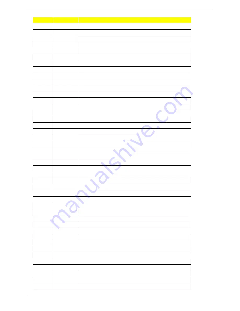
45h
POST device initialization
46h
2-1-2-3
Check ROM copyright notice
48h
Check video configuration against CMOS
49h
Initialize PCI bus and devices
4Ah
Initialize all video adapters in system
4Bh QuietBoot
start
(optional)
4Ch
Shadow video BIOS ROM
4Eh
Display BIOS copyright notice
50h
Display CPU type and speed
51h Initialize
EISA
board
52h Test
keyboard
54h
Set key click if enabled
58h
2-2-3-1
Test for unexpected interrupts
59h
Initialize POST display service
5Ah
Display prompt "Press F2 to enter SETUP"
5Bh
Disable CPU cache
5Ch
Test RAM between 512 and 640 KB
60h
Test extended memory
62h
Test extended memory address lines
64h Jump
to
UserPatch1
66h
Configure advanced cache registers
67h
Initialize Multi Processor APIC
68h
Enable external and CPU caches
69h
Setup System Management Mode (SMM) area
6Ah
Display external L2 cache size
6Bh
Load custom defaults (optional)
6Ch
Display shadow-area message
6Eh
Display possible high address for UMB recovery
70h
Display error messages
72h
Check for configuration errors
76h
Check for keyboard errors
7Ch
Set up hardware interrupt vectors
7Eh
Initialize coprocessor if present
80h
Disable onboard Super I/O ports and IRQs
81h
Late POST device initialization
82h
Detect and install external RS232 ports
83h
Configure non-MCD IDE controllers
84h
Detect and install external parallel ports
85h
Initialize PC-compatible PnP ISA devices
86h
Re-initialize onboard I/O ports.
87h
Configure Mainboard Configurable Devices (optional)
88h
Initialize BIOS Data Area
89h
Enable Non-Maskable Interrupts (NMIs)
Code
Beeps
POST Routine Description
Summary of Contents for Ferrari One 200
Page 2: ...ii PRINTED IN TAIWAN ...
Page 10: ...x Table of Contents ...
Page 13: ...Chapter 1 3 System Block Diagram ...
Page 48: ...38 Chapter 2 ...
Page 60: ...50 Chapter 3 5 Lift the memory card out 6 Repeat steps 4 and 5 for the second memory card ...
Page 63: ...Chapter 3 53 8 Remove the WLAN module ...
Page 74: ...64 Chapter 3 8 Lift the button board away ...
Page 78: ...68 Chapter 3 8 Lift the I O board up by the inner edge and pull away on the angle ...
Page 82: ...72 Chapter 3 7 Lift out the main board from the inside edge ...
Page 84: ...74 Chapter 3 4 Lift the fan away from the main board ...
Page 86: ...76 Chapter 3 2 Lift the RTC battery out of its holder ...
Page 88: ...78 Chapter 3 4 Lift the speaker module out of the lower cover ...
Page 90: ...80 Chapter 3 LCD Bracket Disassembly 2 2 5 4 86 TPK07 001 Step Screw Quantity Part No ...
Page 95: ...Chapter 3 85 4 Lift the LCD panel out of the LCD module ...
Page 100: ...90 Chapter 3 4 Remove the magnet 5 Pull the foil and antennas off the adhesive ...
Page 108: ...98 Chapter 3 2 Press the bezel down around the edges ...
Page 125: ...Chapter 3 115 5 Connect the IO cable to the IO card and main board ...
Page 129: ...Chapter 3 119 2 Press the DIMM module down Replacing the 3G Module 1 Insert the 3G module ...
Page 135: ...Chapter 3 125 Replacing the Dummy Card 1 Insert the dummy card until it clicks into place ...
Page 136: ...126 Chapter 3 ...
Page 156: ...146 Chapter 5 ...
Page 168: ...158 Chapter 6 ...
Page 180: ...170 ...
Page 183: ...173 ...
Page 184: ...174 ...