background image

O n b o a r d  C o n n e c t o r s

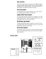
The PR5 has onboard connector headers for the disk con-
trollers, I/O ports, system enclosure connections and sev-
eral other features. Pin 1 locations are noted for cable ori-
entation.

Drive Controller & I/O Port Connectors

The PR5 has floppy disk drive, Enhanced IDE controller,
serial, parallel and USB port connector headers onboard.

Drive Controller Connectors

The Floppy Disk Drive Controller connector is a 34-pin
header. The two Enhanced IDE Controller connectors for
Channel 1 and Channel 2 are 40-pin headers. Ribbon
cables are supplied for each connector. W hen installing
drives, make sure the colored edge of the drive’ s ribbon
cable is at the Pin 1 end of the both the onboard connec-
tor and the drive. Their positions and Pin 1 locations are
shown below.

F D C

I D E 1

I D E 2

Controller Connector Locations

Summary of Contents for PR5

Page 1: ...erence will not occur in a particular installation If this equipment does cause harmful interference to radio or television reception which can be determined by turning the equipment off and on the user is encouraged to try to correct the interference by one or more of the following measures Reorient or relocate the receiving antenna Increase the distance between the equipment and receiver Connect...

Page 2: ...ange The manufacturer reserves the right to alter the contents of this publication at any time and without notice The contents of this publication may contain inaccuracies or typographical errors and is supplied for informational use only Products are noted in this publication for identification purposes only Microsoft is a registered trademark and Windows is a trademark of Microsoft Corporation P...

Page 3: ... Connectors 2 14 Power Input Connector 2 14 Keyboard PS 2 Mouse Connectors 2 14 IDE Activity LED Connector 2 14 CPU Fan Power Connector 2 14 PR5 Hardware Configuration 2 16 CPU Options Installation 2 16 Related Terminology 2 16 CPU Settings 2 18 System Memory Configuration 2 26 DIMM Voltage Settings 2 29 Installing Memory Modules 2 30 Level 2 Cache Options 2 32 Onboard Connectors 2 33 Disk Drive C...

Page 4: ...3 Password Setting 3 24 IDE HDD Auto Detection 3 25 HDD Low Level Format 3 25 Save And Exit Setup 3 25 Exit Without Saving 3 25 Updating The BIOS 3 25 IDE Driver Disk 3 25 Technical Information 4 1 CPU Specifications 4 1 Intel CPUs 4 2 AMD K5 CPUs 4 9 Cyrix CPUs 4 10 IDE Installation Guide 4 11 IDE Transfer Modes 4 11 Installing IDE Devices 4 12 IDE Cables 4 12 Example IDE Configurations 4 12 BIOS...

Page 5: ... section appears in the sidebar on the first page The manual is divided into four sections Section 1 Introduction Section 2 Hardware Configuration Section 3 Software Configuration Section 4 Technical Information Illustrations and tables identify locations and settings and sidebar notes and pointers are used to highlight impor tant information Sidebar Notes Summary information tips and important po...

Page 6: ...ler connector headers on the mainboard This is explained in Section 2 The Support Disk has drivers for use with various oper ating systems These are covered in Section 3 Feature Summary The PR5 mainboard incorporates a variety of perfor mance enhancing features and is designed for use in File Server and Workstation computers and other high end applications It uses Intel s 430VX chipset its PCI exp...

Page 7: ... memory modules Supports Intel specified 3 3V Unbuffered DRAM for DIMM modules System BIOS Award BIOS with support for Plug and Play Advanced Power Management DMI Desktop Management Interface features in cluding system suspend Onboard Multi I O Onboard I O ports and disk con trollers including Two Universal Serial Bus USB ports One EPP ECP bidirectional parallel port Two high speed 16550 compatibl...

Page 8: ...scharge can deliver a high voltage shock to the mainboard sufficient to damage or destroy com ponents on the board Because of this it is important to observe precautions when you handle the mainboard and any devices you install on it including the CPU memory modules and expansion cards There are several simple precautions you can take Use an anti static wrist strap which can be pur chased inexpens...

Page 9: ...AB PR5 PCI Mainboard Layout 1 2 3 4 5 6 7 8 PB SRAM PB SRAM 438VX 438VX 82437VX 8 23 7 1 PIIX3 Pentium CP U Ultra I O 9 1 0 1 1 1 2 1 3 1 4 1 5 1 6 ...

Page 10: ...System Block Diagram ...

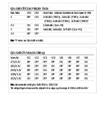
Page 11: ...re are several CPU configuration settings required including CPU voltage External Clock Frequency and External Clock Factor Detailed CPU reference informa tion is in Section 4 CPU Voltage The following charts show the CPU voltage DIP switch settings for Intel AMD and Cyrix CPUs Reference in formation on required voltages is in Section 4 CPU Voltage Settings You must set the CPU voltage using DIP s...

Page 12: ... N OFF 2 93V 3 38V OFF OFF O N OFF OFF OFF O N OFF 3 38V 3 3V OFF O N OFF OFF OFF OFF OFF O N 3 52V 3 3V O N OFF OFF OFF OFF OFF OFF O N Note The factory default Vcore setting is 3 38V The voltage figures shown are the mid point of a range e g the range of 3 52V is 3 45V to 3 6V Cyrix 6x86 CPU Vcore Vio Settings Vcore Vio V C 1 VC2 VC3 VC4 VC5 VC6 VC7 VC8 2 7V 3 3V OFF OFF OFF OFF O N OFF OFF O N ...

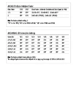
Page 13: ...e The PR5 uses one of several clock generator chips The DS DIP switch block settings vary depending on which chip is installed To determine the correct settings you need to know which clock chip is installed The position of the chip on the mainboard is noted above The chip part information is printed on the top of the chip The options are ICS ICS9159 14 PhaseLink PLL52C59 14T or PLL52C61 01 or PLL...

Page 14: ...O N OFF OFF OFF ON OFF ON OFF O N OFF Clock Chip PLL52C59 14T or ICS9159 14 Ext Clock Factor Ext Clock Freq Norm Turbo ISA Spd Refresh CPU Ext Int Clock D S 1 DS 2 DS 3 DS 4 DS 7 DS 5 DS 6 P75 50 75MHz OFF OFF O N O N OFF ON OFF OFF P90 60 90MHz OFF OFF OFF O N OFF ON O N OFF P100 66 100MHz OFF OFF O N OFF OFF ON O N OFF P120 60 120MHz OFF O N OFF O N OFF ON O N OFF P133 66 133MHz OFF O N O N OFF ...

Page 15: ...z OFF O N OFF OFF ON OFF ON OFF O N OFF Clock Chip PLL52C59 14T or ICS9159 14 Ext Clock Factor Ext Clock Freq Norm Turbo ISA Spd Refresh CPU Ext Int Clock D S 1 DS 2 DS 3 DS 4 DS 7 DS 5 DS 6 PR75 50 75MHz OFF OFF O N O N OFF ON OFF OFF PR90 60 90MHz OFF OFF OFF O N OFF ON O N OFF PR100 66 100MHz OFF OFF O N OFF OFF ON O N OFF PR120 60 90MHz OFF OFF OFF O N OFF ON O N OFF PR133 66 100MHz OFF OFF O ...

Page 16: ...N O F F O F F O N OFF Clock Chip PLL52C59 14T or ICS9159 14 Ext Clock Factor Ext Clock Freq Norm Turbo ISA Spd Refresh CPU Ext Int Clock D S 1 DS 2 DS 3 DS 4 DS 7 DS 5 DS 6 P120 50 100MHz OFF O N O N O N OFF ON OFF OFF P133 55 110MHz OFF O N OFF OFF O F F O N OFF P150 60 120MHz OFF O N OFF O N OFF ON O N OFF P166 66 133MHz OFF O N O N OFF OFF ON O N OFF P200 75 150MHz OFF O N OFF OFF O N O N OFF N...

Page 17: ...2 Bank sequence doesn t matter use any combina tion as long as other requirements are followed DRAM speed must be at least 70ns can be faster Parity checking is not supported Maximum 128MB supported There are numerous allowable memory configurations Since bank sequence is not important as long as you use SIMMs in pairs you can use any combination of banks However for maximum performance it best to...

Page 18: ... of the DRAM on any DIMM modules you install The jumper settings are shown below x x x DIMM Voltage Settings Jumper JP11 sets the voltage sup plied to the DIMM sockets FP EDO modules use the 5 Volt setting Default Setting 3 Volt JP11 DIMM Voltage Pins 1 2 Pins 2 3 5 Volt DIMM Short N A 3 Volt DIMM N A Short Default Note 5 Volt FP or EDO DRAM 3 Volt 3 3 Volt Unbuffered DRAM J P 1 1 Jumper JP11 Loca...

Page 19: ...and USB port connector headers onboard Drive Controller Connectors The Floppy Disk Drive Controller connector is a 34 pin header The two Enhanced IDE Controller connectors for Channel 1 and Channel 2 are 40 pin headers Ribbon cables are supplied for each connector When installing drives make sure the colored edge of the drive s ribbon cable is at the Pin 1 end of the both the onboard connec tor an...

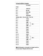
Page 20: ...ts are shown in the table on page 2 11 I O Port Connectors There are five connectors JP2 Infrared port 5 pin USB USB ports 16 pin COM1 COM1 serial port 10 pin COM2 COM2 serial port 10 pin LPT LPT1 printer port 26 pin Pin 1 Upper left hand corner for USB upper right hand corner for COM LPT as shown at right US B C O M 1 COM 2 LPT I O Port Connector Locations x x x x x JP2 IR Connector Pin 1 Connect...

Page 21: ...USB 2 Pins 9 16 Pin 1 5 Volts Pin 2 Ground Pin 3 USBP0 Pin 4 Ground Pin 5 USBP0 Pin 6 Ground Pin 7 Ground Pin 8 Ground Pin 9 5 Volts Pin 10 Ground Pin 11 USBP0 Pin 12 Ground Pin 13 USBP0 Pin 14 Ground Pin 15 Ground Pin 16 Ground Note The USB connector is for two ports Pins 1 through 8 are for the first port and pins 9 through 16 are for the second USB 1 USB 2 ...

Page 22: ...t have all of these fea tures The location of the connector block and the pin assignments are shown below Enclosure Connectors There are five connectors in the block the other pins are unused Reset Pins 1 2 1 Suspend Switch Pins 6 7 2 Turbo LED Pins 8 9 3 Speaker Pins 11 14 4 Keylock Pins 16 20 5 Connectors are labeled at right x x x x x x x x x x x x x x x x x x x x 1 2 3 4 5 Enclosure Features C...

Page 23: ... Sound signal Keylock Power LED Connector Pin 16 Ground Pin 17 Keyboard inhibit signal Pin 18 Ground Pin 19 Unused Pin 20 5 Volts DC for Power LED Note Pins 3 4 5 10 15 are unused Enclosure Features Connectors Not every pin in the connector block for system case features is used Which features are used depends on the spe cific case design If your case does not have a Keyboard Lock you can still co...

Page 24: ...eyboard connector is a standard AT DIN keyboard connector The PS 2 mouse connector is a 6 pin header block for a PS 2 mouse port IDE LED Activity Light Connector The IDE LED activity light connector is a 4 pin connec tor header which will accept either a 2 pin or 4 pin IDE LED activity light connector lead CPU Fan Power Connector The CPU fan power connector is a 3 pin connector header which will a...

Page 25: ...IDE Activity LED Connector J5 Pin 1 Positive cathode pin Pin 2 Negative anode pin Pin 3 Negative anode pin Pin 4 Positive cathode pin CPU Fan Power Connector JP9 Pin 1 Ground Pin 2 12 Volts DC for fan power Pin 3 Ground Power Supply Lead Connectors Some system power supplies have two leads that connect to the J1 power in put connector If this is the case you must connect the power supply leads so ...

Page 26: ...ion Quick Reference So these sections provide additional detail with some review CPU Options Installation The PR5 supports a wide assortment of CPU chips from various manufacturers It is also designed to provide as much upgradability as current information on future CPUs allows We must note however that only the CPUs listed in the manual have been certified to work with the PR5 Related Terminology...

Page 27: ...iplier Factor For example the Intel Pentium P150 CPU has a 150MHz internal clock speed a 2 5 multiple of the 60MHz external clock Clock Multiplier Factor The clock multiplier factor is the factor by which the external clock is multiplied to set the CPU s internal clock speed The PR5 has four options 1 5 2 2 5 3 For example the Pentium P166 requires a 66MHz external clock and a 2 5 clock multiplier...

Page 28: ...et the Clock Multiplier Factor using switches DS1 and DS2 on the DS DIP switch block 2 Set the External Clock configuration using switches DS3 DS4 and DS7 on the DS DIP switch block 3 Set the ISA Bus Clock configuration using switch DS5 on the DS DIP switch block 4 Make sure DS6 on the DS DIP switch block is OFF This controls DRAM refresh and is reserved for use with future CPUs The default settin...

Page 29: ... 6 25MHz Off 8 3 3 M H z 60MHz O n 7 5 M H z Off 10 MH z 66MHz O n 8 2 5 M H z Off 1 1 M H z Note The suggested setting is highlighted in bold face type in the chart DS5 ON ISA Bus Clock External Clock 8 DS5 OFF ISA Bus Clock External Clock 6 Factory default setting is ON 1 2 3 4 5 6 7 8 ON DIP 1 2 3 4 5 6 7 8 ON DIP ...

Page 30: ...default setting 2 The internal clock speed also indicates which Pentium it is for e g 75 is for P75 90 is for P90 etc Intel Pentium CPU Vcore Vio Settings Vcore Vio V C 1 VC2 VC3 VC4 VC5 VC6 VC7 VC8 2 7V 3 3V OFF OFF OFF OFF O N OFF OFF O N 2 8V 3 3V OFF OFF OFF O N OFF OFF OFF O N 2 93V 3 3V OFF OFF O N OFF OFF OFF OFF O N 3 38V 3 3V OFF O N OFF OFF OFF OFF OFF O N 3 52V 3 3V O N OFF OFF OFF OFF ...

Page 31: ...O N OFF OFF OFF ON OFF ON OFF O N OFF Clock Chip PLL52C59 14T or ICS9159 14 Ext Clock Factor Ext Clock Freq Norm Turbo ISA Spd Refresh CPU Ext Int Clock D S 1 DS 2 DS 3 DS 4 DS 7 DS 5 DS 6 P75 50 75MHz OFF OFF O N O N OFF ON OFF OFF P90 60 90MHz OFF OFF OFF O N OFF ON O N OFF P100 66 100MHz OFF OFF O N OFF OFF ON O N OFF P120 60 120MHz OFF O N OFF O N OFF ON O N OFF P133 66 133MHz OFF O N O N OFF ...

Page 32: ...R120 100 is for PR100 and PR133 AMD AMD K5 CPU Vcore Vio Settings Vcore Vio V C 1 VC2 VC3 VC4 VC5 VC6 VC7 VC8 2 7V 3 38V OFF OFF OFF OFF O N OFF O N OFF 2 8V 3 38V OFF OFF OFF O N OFF OFF O N OFF 2 93V 3 38V OFF OFF O N OFF OFF OFF O N OFF 3 38V 3 3V OFF O N OFF OFF OFF OFF OFF O N 3 52V 3 3V O N OFF OFF OFF OFF OFF OFF O N Note The factory default Vcore setting is 3 38V The voltage figures shown ...

Page 33: ...z OFF O N OFF OFF ON OFF ON OFF O N OFF Clock Chip PLL52C59 14T or ICS9159 14 Ext Clock Factor Ext Clock Freq Norm Turbo ISA Spd Refresh CPU Ext Int Clock D S 1 DS 2 DS 3 DS 4 DS 7 DS 5 DS 6 PR75 50 75MHz OFF OFF O N O N OFF ON OFF OFF PR90 60 90MHz OFF OFF OFF O N OFF ON O N OFF PR100 66 100MHz OFF OFF O N OFF OFF ON O N OFF PR120 60 90MHz OFF OFF OFF O N OFF ON O N OFF PR133 66 100MHz OFF OFF O ...

Page 34: ...OFF OFF Note P series are Cyrix 6x86 or 6x86L Cyrix 6x86 CPU Vcore Vio Settings Vcore Vio V C 1 VC2 VC3 VC4 VC5 VC6 VC7 VC8 2 7V 3 3V OFF OFF OFF OFF O N OFF OFF O N 2 8V 3 3V OFF OFF OFF O N OFF OFF OFF O N 2 93V 3 3V OFF OFF O N OFF OFF OFF OFF O N 3 38V 3 3V OFF O N OFF OFF OFF OFF OFF O N 3 52V 3 3V O N OFF OFF OFF OFF OFF OFF O N Note Recommended setting for 6x86 CPUs is 3 52V 3 3V The voltag...

Page 35: ...N O F F O F F O N OFF Clock Chip PLL52C59 14T or ICS9159 14 Ext Clock Factor Ext Clock Freq Norm Turbo ISA Spd Refresh CPU Ext Int Clock D S 1 DS 2 DS 3 DS 4 DS 7 DS 5 DS 6 P120 50 100MHz OFF O N O N O N OFF ON OFF OFF P133 55 110MHz OFF O N OFF OFF O F F O N OFF P150 60 120MHz OFF O N OFF O N OFF ON O N OFF P166 66 133MHz OFF O N O N OFF OFF ON O N OFF P200 75 150MHz OFF O N OFF OFF O N O N OFF N...

Page 36: ...s on the PR5 mainboard Pentium type CPUs are 64 bit CPUs This has a direct effect on the memory design Since 72 pin SIMM sock ets are 32 bit they have to be used in pairs to create a 64 bit data path This means that SIMM modules have to be installed in pairs The four SIMM sockets on the PR5 are therefore divided into banks of two sockets each re sulting in two banks Because DIMM sockets are 64 bit...

Page 37: ...t 70ns can be faster Parity checking is not supported Maximum 128MB supported There are numerous allowable memory configurations Since bank sequence is not important as long as you use SIMMs in pairs you can use any combination of banks However for maximum performance it best to use the same type of DRAM in all banks SDRAM provides higher performance than EDO DRAM and EDO is faster than Fast Page ...

Page 38: ...Note the 2 sided module restriction SIMM Banks You can install memory in bank SIMM1 2 only SIMM2 3 only or both banks The bank order doesn t matter You must install two modules of the same size type and speed in a bank You can mix different sizes between banks in any combination as long as the total doesn t exceed 128MB You can even install different DRAM types in between banks FP or EDO DIMM Bank...

Page 39: ...t match the voltage of the DRAM on any DIMM modules you install The jumper settings are shown below x x x DIMM Voltage Settings Jumper JP11 sets the voltage sup plied to the DIMM sockets Default Setting 3 Volt JP11 DIMM Voltage Pins 1 2 Pins 2 3 5 Volt DIMM Short N A 3 Volt DIMM N A Short Default Note 5 Volt FP or EDO DRAM 3 Volt 3 3 Volt Unbuffered DRAM J P 1 1 Jumper JP11 Location Pin 1 ...

Page 40: ... before you can insert them in the socket SIMM and DIMM modules have different designs for ensuring correct mod ule orientation SIMM modules have one lower corner cut away to en sure they will only insert in a socket in the correct orien tation The SIMM sockets have an extension from one of the socket guide posts that prevents the module from in serting in the socket if it isn t oriented correctly...

Page 41: ...Insert the module edge into the socket at a 90 angle so that the contacts insert as far as they will go 3 The retaining clamps at each end rotate upward to secure the module in the socket The figure below shows where the orientation features are located DIMM module orientation short connector SIMM module cut away corner goes at this end Memory Module Orientation ...

Page 42: ...el 2 cache on the PR5 greatly speeds up system operation There will be at least 256KB of very fast Pipe line Burst Static RAM SRAM cache memory mounted either on the mainboard or on a cache module that in stalls in the cache socket You can upgrade the Level 2 cache to a maximum of 512KB regardless of whether the memory is on the board or on a module If there is 256KB of cache memory mounted on the...

Page 43: ...so has I O Input Output ports built in in cluding serial parallel and USB port connectors onboard External ports connect to the onboard connectors via the cables attached to ports Drive Controller Connectors The PR5 comes with ribbon cables to connect your sys tem floppy disk and IDE drives to the mainboard The cables are colored on one edge to show you how to ori ent the cable That edge of the ca...

Page 44: ...O Port Connectors The PR5 has two serial ports a parallel port an infrared port and a dual port USB connector onboard Combina tion ribbon cable to external port cables are supplied for each connector except the infrared port The I O ports enable you to connect external devices such as modems and printers to your system The serial ports are the COM1 and COM2 ports and the parallel port is the LPT1 ...

Page 45: ...or The system power supply connector is a 12 pin connec tor divided into two sections P8 and P9 The leads from the system power supply plug onto this connector and snap into place If you connect the leads yourself make sure you plug them on so that the black wires on each lead are in the middle of the connector Keyboard PS 2 Mouse Connectors The external keyboard connector is a standard AT DIN key...

Page 46: ...Assignments Pin Function AT Keyboard Pin 1 Keyboard Clock Pin 2 Keyboard Data Pin 3 Not used Pin 4 Ground Pin 5 5 Volts DC PS 2 Port Pin 1 Mouse Data Pin 2 Not used Pin 3 Ground Pin 4 5 Volts DC Pin 5 Mouse Clock Pin 6 Not Used ...

Page 47: ...erence if you need them CPU Fan Power Connector The CPU fan power connector is a 3 pin connector header which will accept either a 2 pin or 3 pin CPU fan power lead connector Some CPU fans have a connector for a standard power lead from the system power supply If your CPU fan is attached to the top of the CPU chip as with some Intel Pentiums the power lead connector should fit this onboard connect...

Page 48: ...P Block Switch 1 External Clock Factor Switch 2 External Clock Factor Switch 3 External Clock Frequency Switch 4 External Clock Frequency Switch 5 ISA Bus Clock Switch 6 DRAM Refresh Switch 7 External Clock Frequency Switch 8 Reserved VC DIP Block Pin 1 8 Vcore Vio voltage settings Jumpers JP1 L2 Cache JP3 Clear CMOS JP8 Flash ROM Type JP10 Reserved JP 11 DIMM Voltage ...

Page 49: ...pens you must clear erase the CMOS memory and enter new configuration informa tion in the BIOS Setup program The BIOS Setup pro gram is covered in Section 3 To clear the CMOS memory do as follows 1 Remove the jumper cap from Pins 1 2 2 Place the cap over Pins 2 3 for five seconds 3 Replace the cap over Pins 1 2 When you are done you can start up your computer and run the Setup program to re enter ...

Page 50: ...chip 5 Volt and 12 Volt The chip type has no functional effect The settings and location are shown below JP8 Flash Chip Type This jumper is factory set for the type of Flash Memory Chip installed The jumper may not be present on some boards with the setting hardwired on the board instead Jumper JP8 Location JP8 Flash Type Pin 1 JP8 Flash Memory Chip Type Pins 1 2 Pins 2 3 5 Volt Chip Short 12 Volt...

Page 51: ...ns This section is made up of tables and diagrams designed to help you identify the CPU you want to install You need to identify your CPU in order to determine the cor rect configuration settings CPU s from Intel AMD and Cyrix are covered here CPUs vary within a specific type a 120MHz Pentium for ex ample can have different power and timing specifica tions depending on which type and Step version ...

Page 52: ...m valid delay AC timing for some signals KIT Supports timing for C55 C88 cache chipsets Also please note the following P54C Beginning with the P54C E Step Standard timing was replaced by existing Min Delay timing P54CS P54CS PPGA UP No DP No APIC No FRC Beginning with the P54C E Step Standard timing was replaced by existing Min Delay timing P55C P55C A Step is NOT a production stepping A 1 Step Vc...

Page 53: ...dware including the disk drives installed system memory and video display It also records system customization information and settings for the main board s chipset power management and configurable hardware In addition the Setup program has a Password feature automatic hard disk detection and a hard disk low level format command Accessing The CMOS Setup Utility When you turn on your computer a me...

Page 54: ...ain Menu Menu Commands If you look at the lower portion of the screen illustration you ll see a section that lists the control commands for this level of the program You execute a command by pressing the key for that command The program com mands are Qu it This command will close the Setup program when you press the ESC key Save Exit Setup This will save the current settings and close the Setup pr...

Page 55: ...up the green power management features PCI Onboard I O Setup PCI expansion bus and drive controller settings serial parallel and IR port settings The other main menu items interact with these main sections Load BIOS Defaults Loads minimum settings from the BIOS ROM Load Setup Defaults Loads standard settings from the BIOS ROM Password Setting Sets system password which is configured by the Securit...

Page 56: ...the arrow keys on your keyboard to move around the screen and select a menu item An item is highlighted when it is selected Change Color You can change the program color scheme by press ing Shift F2 Award BIOS Standard CMOS Setup Base Memory 640K Extended Memory 7168K Other Memory 384K Total Memory 8192K Date mm dd yy Wed Aug 21 1996 Time hh mm ss 10 30 00 HARD DISKS TYPE SIZE CYLS HEADS PRECOMP L...

Page 57: ...necessary Date Time The first two lines on the screen are the date and time settings for the system clock Hard Disk Type Parameters Use the IDE HDD Auto Detection feature to automati cally enter the drive parameters of IDE hard disk drives in these fields If you have only SCSI hard disk drives installed in your system leave the settings here at None Only hard disk information needs to be entered h...

Page 58: ...l physical address The maximum drive size supported is 8 4GB Large For 1GB or smaller drives with more than 1024 cyl inders and no LBA support This access mode causes the Operating System to treat the drive as if it has fewer than 1024 cylinders by dividing the cylinder total in half and doubling the number of heads Drives needing this mode are less common Most large IDE hard disk drives currently...

Page 59: ...ding to the type of display card in your system This should normally be left on EGA VGA The options are EGA VGA Mono for Hercules or MDA CGA 40 CGA 80 Error Handling The last line Halt On sets when the system stops if an error occurs The options are All Errors Default No Errors All But Keyboard All But Diskette All But Disk Key When you are finished in this section exit to the main menu screen by ...

Page 60: ...menu item An item is highlighted when it is selected Award BIOS BIOS Features Setup Virus Warning Disabled CPU Internal Cache Enabled External Cache Enabled Quick Power On Self Test Enabled Boot Sequence A C Swap Floppy Drive Disabled Boot Up Floppy seek Disabled Boot Up NumLock Status On IDE HDD Block Mode Enabled Typematic Rate Setting Enabled Typematic Rate Chars Sec 30 Typematic Delay Msec 250...

Page 61: ... your mainboard is already installed in a working sys tem the proper entries are already entered on this screen and you shouldn t change them Virus Warning This protects the primary hard disk s boot sector and par tition table from infection Any attempt to write to them will halt the system and produce a warning message If this happens you can either allow the system to con tinue or stop it and bo...

Page 62: ...ptions are A C C A C CD ROM A CD ROM C A Swap Floppy Drive This switches the floppy drive assignments so that drive A is treated as drive B and drive B as drive A under DOS The default setting is Disabled Boot Up Floppy Seek When enabled the BIOS checks the floppy disk drive s to see if they are 40 track 360KB floppy disk drive or 80 track all other types Don t enable this unless your system has a...

Page 63: ...erval the time between the display of one character and the next There are four delay rate choices measured in milliseconds 250 500 750 and 1000 The default is 250 Security Option This sets when password protection is used The two options are System Password required at boot up Setup Password controls access to Setup utility You create a password using the Password Setting op tion in the main menu...

Page 64: ...dowing other expansion card ROMs If there are any expansion cards with ROMs installed in your system you have to know the address range they use to shadow them specifically The default setting for all of these is Disabled When you are done in this section press the Esc key to return to the main menu The Shadow Feature The term Shadow mentioned at right refers to a performance enhancement feature w...

Page 65: ...led ROM PCI ISA BIOS XXXXXXXX CHIPSET FEATURES SETUP AWARD SOFTWARE INC ESC Quit F1 Help F5 Old Values F6 Load BIOS Defaults F7 Load Setup Defaults Select Item PU PD Modify SHIFT F2 Color Menu Commands The menu commands for this screen are the same as for the BIOS Features Setup screen Auto Configuration Everything on this screen except for the Memory Hole item is set automatically when auto confi...

Page 66: ...Management Setup To enter this section of the Setup program highlight this menu item in the main menu and press the Enter key The following screen will appear Award BIOS Power Management Setup Menu Commands The menu commands for this screen are the same as for the BIOS Features Setup screen What Power Management Does Power management lets you set up your computer to save electricity when it is not...

Page 67: ... set to Yes the Advanced Power Manage ment feature in Microsoft Windows controls power man agement operation The default setting is No Video Off Method This governs monitor power saving by controlling how power management blanks the monitor screen The de fault setting blanks the screen and turns off vertical and horizontal scanning and requires a monitor with green features If you don t have this ...

Page 68: ...aving mode power man agement will skip to the next mode in the sequence if this is disabled Standby Mode This sets the period of system inactivity after which the system goes into Standby mode the intermediate power saving state The settings range from 1 minute to 1 hour and can be set manually when power management is in User Define mode The default setting is Disabled When the system goes into p...

Page 69: ...Standby The system will resume from Doze or Standby mode if there is any activity by the parts of the system that use the IRQs listed in this section when they are set to ON The system won t wake up from such activity if an item is set to OFF The default settings are set so that the sys tem will respond to mouse or modem activity The de fault settings are IRQ3 Wake Up Event O N IRQ4 Wake Up Event ...

Page 70: ...hannel Enabled PCI IDE Card IRQ Map to PCI AUTO Primary IDE INT A Secondary IDE INT B PS 2 Mouse Function IRQ12 Enable Onboard IDE 1 Controller Enable Master Drive PIO Mode AUTO Slave Drive PIO Mode AUTO Onboard IDE 2 Controller Enable Master Drive PIO Mode AUTO Slave Drive PIO Mode AUTO Menu Commands The menu commands for this screen are the same as for the BIOS Features Setup screen PCI PnP BIOS...

Page 71: ...er which slot it is installed in by selecting the slot number IRQ14 will be as signed automatically ISA This for PCI IDE cards that connect to IRQs 14 and 15 directly via a paddleboard installed in an ISA slot and connected to the card by a cable No IRQ is assigned to the slot with the PCI IDE card in it The PCI Slot INT specification options are Slot1 INT A Slot2 INT B Slot3 INT C Slot4 INT D Slo...

Page 72: ... disk drive controller on and off The default setting is Enabled Onboard Serial Ports 1 2 These two lines set the address and IRQ assignment or disable the onboard serial ports The default settings are the standard assignments for these ports You can choose another option or disable them if you want Don t use the same settings for both ports The settings are as fol lows Serial Port 1 3F8 IRQ4 Defa...

Page 73: ...ult setting is Hi Hi Onboard Parallel Port This sets the address and IRQ assignment or disables the onboard parallel port The default setting is the standard assignment for parallel ports You can choose another op tion if you want The default setting is 378 IRQ7 Parallel Port Mode The onboard parallel port supports standard EPP and ECP modes The default setting is Normal SPP The options are as fol...

Page 74: ...o load the BIOS defaults Press the Y key and then the Enter key The BIOS default settings will load Press the N key if you want to cancel Award BIOS Load BIOS Defaults ROM PCI ISA BIOS XXXXXXXX CMOS SETUP UTILITY AWARD SOFTWARE INC Load BIOS Defaults Y N N ESC Quit F10 Save Exit Setup Select Item SHIFT F2 Change Color Load BIOS Defaults except Standard CMOS SETUP This loads a set of troubleshootin...

Page 75: ... to load the Setup defaults Press the Y key and then the Enter key The Setup default settings will load Press the N key if you want to cancel This loads a set of optimized default values permanently stored in the BIOS ROM Use this command to load de fault settings for normal system operation Standard CMOS Setup is not affected by this command Award BIOS Load Setup Defaults ESC Quit F10 Save Exit S...

Page 76: ...ype in a password The password is case sensitive and can be up to 8 alphanumeric characters Press Enter when you finish typing in the password If you typed in a password the message Confirm Pass word will appear Confirm the password by typing it again and pressing Enter The message box will close If you don t want to set a password after you invoke this command or if you want to eliminate an exist...

Page 77: ...ed again Low level formatting is not the same as the formatting you perform when installing an operating system In the event that you need to use this utility the drive you use it on must be set to Normal mode in Standard CMOS Setup Save And Exit Setup When you select this and press Enter the values entered during the current session are recorded in CMOS memory Exit Without Saving When you select ...

Page 78: ...ns This section is made up of tables and diagrams designed to help you identify the CPU you want to install You need to identify your CPU in order to determine the cor rect configuration settings CPU s from Intel AMD and Cyrix are covered here CPUs vary within a specific type a 120MHz Pentium for ex ample can have different power and timing specifica tions depending on which type and Step version ...

Page 79: ...m valid delay AC timing for some signals KIT Supports timing for C55 C88 cache chipsets Also please note the following P54C Beginning with the P54C E Step Standard timing was replaced by existing Min Delay timing P54CS P54CS PPGA UP No DP No APIC No FRC Beginning with the P54C E Step Standard timing was replaced by existing Min Delay timing P55C P55C A Step is NOT a production stepping A 1 Step Vc...

Page 80: ... STD Yes E 0 P54C SY005 75MHz 1 5 50MHz STD STD STD Yes E 0 90MHz Pentium C P U Internal Bus External Power C P U D P C P U Type Spec Clock Factor Clock Vcore Vio Timing Supp Step Comment P54C Sx653 90MHz 1 5 60MHz STD STD STD Yes B 5 P54C Sx957 90MHz 1 5 60MHz STD STD STD Yes B 5 P54C Q0654 90MHz 1 5 60MHz VR VR STD Yes B 5 P54C Sx958 90MHz 1 5 60MHz VR VR STD Yes B 5 P54C Q0655 90MHz 1 5 60MHz S...

Page 81: ... VRE VRE M D N o B 3 P54C Q0656 100MHz 1 5 66MHz STD STD STD Yes B 5 P54C Q0657 100MHz 1 5 66MHz VR VR M D N o B 5 P54C Q0658 100MHz 1 5 66MHz VRE VRE M D Yes B 5 P54C Sx962 100MHz 1 5 66MHz VRE VRE M D Yes B 5 P54C Q0698 S100MHz 1 5 66MHz VRE VRE M D Yes C 2 P54C Q0697 S100MHz 1 5 66MHz STD STD STD Yes C 2 P54C Sx963 100MHz 1 5 66MHz STD STD STD Yes C 2 P54C Sx970 100MHz 1 5 66MHz VRE VRE M D Yes...

Page 82: ... Yes B 5 P54CQS Q 0 7 1 1 120MHz 2 60MHz VRE VRE M D Yes C 2 Convert to P54C P54CQS Q0730 120MHz 2 60MHz STD STD M D Yes C 2 P54CQS Sk084 120MHz 2 60MHz STD STD M D Yes C 2 P54CQS Sk086 120MHz 2 60MHz VRE VRE M D Yes C 2 Convert to P54C P54C Sx994 120MHz 2 60MHz VRE VRE M D N o C 2 P54C Q0732 S120MHz 2 60MHz VRE VRE M D N o C 2 P54C Q0785 120MHz 2 60MHz VRE VRE STD N o E 0 P54C SY008 120MHz 2 60MH...

Page 83: ...TD STD STD Yes B 1 P54CS S106J 133MHz 2 66MHz STD STD STD Yes B 1 P54CS Sk107 133MHz 2 66MHz STD STD Kit Yes B 1 P54CS Q0843 133MHz 2 66MHz STD STD STD Yes C 0 P54CS SY022 133MHz 2 66MHz STD STD STD Yes C 0 P54CS Q0844 133MHz 2 66MHz STD STD Kit Yes C 0 P54CS SY023 133MHz 2 66MHz STD STD Kit Yes C 0 P54CQS Q0733 133MHz 2 66MHz STD STD M D Yes C 2 Convert to P54CS P54CQS Sk098 133MHz 2 66MHz STD ST...

Page 84: ...35 150MHz 2 5 60MHz STD STD STD Yes C 0 P54CS S Y0 15 150MHz 2 5 60MHz STD STD STD Yes C 0 P54CS Q0878 150MHz 2 5 60MHz STD STD STD Yes C 0 PPGA P55C Q0939 150MHz 2 5 60MHz 2 9V 3 3V A 1 CPGA P55C Q 0 9 4 1 150MHz 2 5 60MHz 2 9V 3 3V A 1 PPGA P55C Q 9 7 4 150MHz 2 5 60MHz 2 8V 3 3V A 2 CPGA P55C Q 9 7 7 150MHz 2 5 60MHz 2 8V 3 3V A 2 PPGA ...

Page 85: ...es C 0 P54CS Q0886 166MHz 2 5 66MHz VRE VRE STD Yes C 0 PPGA P54CS Q0890 166MHz 2 5 66MHz VRE VRE Kit Yes C 0 PPGA P55C Q0940 166MHz 2 5 66MHz 2 9V 3 3V A 1 CPGA P55C Q0942 166MHz 2 5 66MHz 2 9V 3 3V A 1 PPGA P55C Q 9 7 5 166MHz 2 5 66MHz 2 8V 3 3V A 2 CPGA P55C Q 9 7 8 166MHz 2 5 66MHz 2 8V 3 3V A 2 PPGA P55C Q 0 1 9 166MHz 2 5 66MHz 2 8V 3 3V A 3 PPGA 200MHz Pentium C P U Internal Bus External P...

Page 86: ...ock Speed CPU Model P Rating 75 90 100 120 133 150 166 Package Type A SPGA 296 pin Operating Voltage B 3 45V 3 60V C 3 30V 3 465V F 3 135V 3 465V G x y H 2 86V 3 0V 3 30V 3 465V J 2 57V 2 84V 3 30V 3 465V K 2 38V 2 63V 3 30V 3 465V x Vcore y Vio Reserved Case Temperature Q 60 C R 70 C W 55 C X 65 C Y 75 C Z 85 C AMD K5 CPU Markings ...

Page 87: ...pe 6x86 P166 GP 133MHz Internal Clock Speed Core Frequency 100 110 120 133 150 CPU Model 6x86 6x86L P Rating 90 120 133 150 166 200 Center of Core Voltage 3 3V 3 52V 2 5V 2 7V VCC Specification Full spec 3 15V 3 7V C spec 16 3 15V 3 45V C spec 028 3 4V 3 7V Cyrix 6x86 CPU Markings 3 52V 028 ...

Page 88: ... between the hard disk and the system takes place via one of several transfer modes PIO mode Master mode or DMA mode Master Mode In Master mode when the system reads data the mainboard chipset performs hard disk read opera tions directly using either PIO or DMA and places retrieved data in the system memory PIO Mode Programmed Input Output In PIO mode to read data the CPU issues I O com mands to t...

Page 89: ...inboard Note that one edge of the cable is colored to indicate the Pin 1 side When you connect the cable to the mainboard and a device you must orient the cable so that this colored edge is at the Pin 1 side of the connector you are plugging it on to The cables have three connectors on them one at each end and one in between closer to one of the ends When you install a drive plug the end by itself...

Page 90: ... install it in the system case 3 Plug the other end of the IDE cable onto the IDE1 connector on the mainboard with the Pin 1 posi tions aligned 4 Connect the Master end of the other IDE ribbon cable to the CD ROM drive aligning the Pin 1 po sitions and install it in the system case 5 Plug the other end of the IDE cable onto the IDE2 connector on the mainboard with the Pin 1 posi tions aligned 6 Us...

Page 91: ...IDE ribbon cable to the Master drive aligning the Pin 1 positions and install it in the system case 3 Install the Slave drive in the system case and con nect the IDE ribbon cable s Slave connector to it aligning the Pin 1 positions 4 Plug the other end of the IDE cable onto the IDE1 connector on the mainboard with the Pin 1 posi tions aligned 5 Connect the Master end of the other IDE ribbon cable ...

Page 92: ...nto the IDE1 connector on the mainboard with the Pin 1 posi tions aligned 5 Connect the Master end of the second IDE ribbon cable to the other Master drive aligning the Pin 1 positions and install it in the system case 6 Plug the other end of the IDE cable onto the IDE2 connector on the mainboard with the Pin 1 posi tions aligned 7 Use the BIOS CMOS Setup Utility to enter the drive parameters for ...

Page 93: ... Pin 1 posi tions aligned 5 Connect the Master end of the second IDE ribbon cable to the other Master drive aligning the Pin 1 positions and install it in the system case 6 Install the CD ROM drive in the system case and connect the Slave middle connector of the IDE ribbon cable to it aligning the Pin 1 positions 7 Plug the other end of the second IDE cable onto the IDE2 connector on the mainboard...

Page 94: ...only is it gen erally unnecessary to use the HDD Low Level Format feature of the BIOS CMOS Setup Utility but it is also inadvisable if the drive was formatted with proprietary software You should make sure this is not the case be fore you use this feature The second formatting procedure is part of installing the operating system you will use and also involves parti tioning the drive Since this pro...

Page 95: ...isplay card and see if the system will start If it does please note the display card model mainboard model CPU BIOS identification number and a description of the problem If the system will start Remove all expansion cards except the display card Install the other expansion cards one at a time and see if the system will start after you install each card If the system won t start after you install ...

Page 96: ...ons and help solve problems The form is on the next page 1 Product Model This mainboard is the PR5 2 Product Revision Number The product version The format is x xx e g 2 11 3 BIOS ID The BIOS identification number It is at the end of the line that appears after the Press DEL To Enter Setup message at boot up It looks some thing like this 04 19 96 SiS 5511B 5513 2A5IDA1CC D6 where D6 is the ID numb...

Page 97: ...he manufacturer type size and speed of the installed DRAM For example Panasonic SIMM FP DRAM 4MB 06 or NpNX SIMM EDO DRAM 8MB 06 or SEC DIMM S DRAM 8MB G12 1 0 Coast Cache Module Specifications The manufacturer size and product num ber of the installed COAST cache module For example Winbond 256KB W25P010AF 8 1 1 Installed Add On Cards The specifications and slot occupied for all add on cards for e...

Reviews: