AD8HR
37
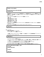
These are results of checks of SRAM (IC010 and IC011) and CPU connections.
The first line shows the D15,D14 ..., D1,D0 status from the left for the data bus.
The second line shows the A15,A14...,A2,A1 (seen from CPU) status from the left for the address bus.
In all cases, correct locations are shown with an O. Error locations are shown with an X.
[2]
FLASH MEMORY (IC013)
This is displayed when W/R check results of the FLASH MEMORY (IC013) were a failure.
[3]
BATTERY
This appears when the voltage of the backup battery is wrong (below 3 volts or above 3.5 volts). This is also
displayed during service test when below 2.5 volts or above 3.5 volts.
[4]
PLLP2 (IC052)
This appears when results of the PLLP2 (IC052) and CPU connection check were NG (failure).
[5]
PLL (IC058, IC059) BNC OUT ->BNC IN
This appears when results of the PLL (IC058 and IC059) check were NG (failure).
This is also displayed when the repeating BNC OUT-> IN loop-back check was NG (failure).
[6]
ATSC2 (IC921)
This appears when the ATSC2 (IC921) and CPU connection check results were NG (failure).
[7]
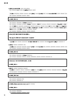
DSP7 (IC902) Data Bus
OOOO OOOO OOOO OOXX
DSP7 (IC902) Chip Select
DSP7 (IC902) Address Bus
OOOO OX X
DSP7 (IC902) SO [24] -> ATSC2 (IC921) PI [A0]
DSP7 (IC902) SO [25] -> ATSC2 (IC921) PI [A1]
DSP7 (IC902) SO [26] -> ATSC2 (IC921) PI [A2]
DSP7 (IC902) SO [27] -> ATSC2 (IC921) PI [A3]
DSP7 (IC902) SO [32] -> ATSC2 (IC921) PI [C0]
DSP7 (IC902) SO [33] -> ATSC2 (IC921) PI [C1]
DSP7 (IC902) SO [34] -> ATSC2 (IC921) PI [C2]
DSP7 (IC902) SO [35] -> ATSC2 (IC921) PI [C3]
This appears when the DSP7 (IC0902) connection check results were NG (failure). OK (pass) items are not
displayed.
The first line shows the D15,D14 ..., D1,D0 status from the left for the data bus.
The third line shows the A7,A6...,A2,A1 (seen from CPU) status from the left for the address bus.
In all cases, correct locations are shown with an O. Error locations are shown with an X.
The second line is displayed when the Chip Select is NG (failure).
The 4th to 11th lines are displayed when the SO->ATSC2 PI connection check for DSP7 (IC902) was NG (fail).
[8]
DIT A (IC903)
This appears when the DIT A (IC903) and CPU connection check results were NG (failure).
[9]
DIT B (IC924)
This appears when the DIT B (IC924) and CPU connection check results were NG (failure).
[10] DIR (IC929)
DIR (IC929) DIGITAL OUT A
The first line appears when the DIR (IC929) and CPU connection check results were NG (failure).
The second line appears when the repeating check results for DIGITAL OUT-> IN was NG (failure).
Содержание AD8HR
Страница 8: ...8 AD8HR CIRCUIT BOARD LAYOUT DC MAIN COMB SW SUB PN PNCOM PNCOM PNCOM PNCOM PNCOM HIC HA ユニットレイアウト ...
Страница 24: ...24 AD8HR MAIN Circuit Board B B 2NAP WC06220 D010 1 ...
Страница 25: ...AD8HR 25 B B Shield MAIN Soldering ハンダ付け シールドMAIN Pattern side 2NAP WC06220 D010 1 パターン側 ...
Страница 26: ...26 AD8HR C C 1 2 3 4 5 6 D D PN Circuit Board E E to MAIN CN982 F F DC Circuit Board 2NAP WC06230 D010 1 ...


