Hardware User Guide
2-6
Xilinx Development System
RD (TDO)
TDI
TCK
TMS
These pins are used for JTAG
Programmer device configura-
tion.
The JTAG/boundary scan pins
function for FPGA and CPLD
JTAG operations.
CLKI-IN
Clock Input — Transmits your
system clock to the MultiLINX
electronic.
Clock must be between 120 kHz
and 10 MHz.
Connect this pin to target system
clock to synchronize the read-
back trigger with target system
clock.
CLK1-OUT
Clock Output — Drives target
system clock.
Clock can come from either the
CLKI-IN pin, or it can be inter-
nally generated by the Multi-
LINX Cable when CLKI-IN is
unconnected.
D0-D7
Data Bus — This pin is used for
Virtex SelectMAP Mode.
An 8 bit data bus supporting the
SelectMAP, and Express configu-
ration modes.
CS0 (CS)
Chip Select — CS on the Virtex;
and CS0 on the XC4000 and
XC5200 FPGAs.
The CS0/CS pin represents a
chip select to the
CS1
Chip Select — The CS1 pin repre-
sents Chip Select to the XC4000
and XC5200 FPGAs during
configuration.
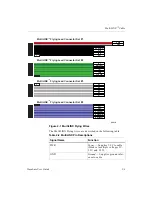
Table 2-2 MultiLINX Pin Descriptions
Signal Name
Function
Содержание MultiLINX DLC4
Страница 2: ...Hardware User Guide ...
Страница 10: ...Hardware User Guide vi Xilinx Development System ...
Страница 38: ...Hardware User Guide 1 24 Xilinx Development System ...
Страница 108: ...Hardware User Guide Glossary 4 Xilinx Development System ...

