Hardware User Guide
3-16
Xilinx Development System
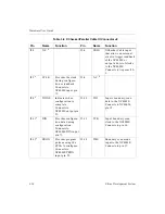
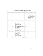
J2-5
N.C.
b
J2-6
TRIG
XChecker Cable input
that allows an external
event to trigger readback
of the XC4003E or
output a burst of clocks
to the XC4003E.
Connects to tiepoint J10–
1.
J2-7
CCLK
Provides the clock
during configura-
tion or readback.
Connects to
XC4003E input pin
73.
J2-8
N.C.
J2-9
DONE
Indicates when
configuration is
complete.
Connects to
XC4003E output pin
53.
J2-10
TDI
Inputs boundary-scan
data to the XC4003E.
Connects to XC4003E
pin 15.
J2-11
DIN
Provides configura-
tion data during
configuration.
Connects to
XC4003E DIN input
pin 71.
J2-12
TCK
Input boundary scan
clock to the XC4003E.
Connects to pin 16.
J2-13
PROG
Provides program
pulse causing the
FPGA to configure.
Connects to
XC4003E PROG
input pin 55.
J2-14
TMS
Boundary scan mode
input to the XC4003E.
Connects to pin 17.
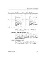
Table 3-6 XChecker/Parallel Cable III Connector J2
Pin
Name
Function
Pin
Name
Function
Содержание MultiLINX DLC4
Страница 2: ...Hardware User Guide ...
Страница 10: ...Hardware User Guide vi Xilinx Development System ...
Страница 38: ...Hardware User Guide 1 24 Xilinx Development System ...
Страница 108: ...Hardware User Guide Glossary 4 Xilinx Development System ...

