background image

Hardware User Guide

1-16

Xilinx Development System

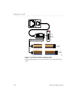
Figure 1-9 XChecker Cable and Flying Leads

The following figure shows top and bottom views of the XChecker
Cable.

Connection to Host Computer

XChecker Cable

Flying Lead Connector 1

Header 1

Header 2

Flying Lead Connector 2

DB25 Adapter

DB9 Socket Connector

+5V

Test Fixture

(Enlarged to
show plugs)

Connections to
Target System

Connections to
Target System

GND

X8322

VCC
GND

CCLK

D/P
DIN

PROG

INIT
RST

TRIG

RD

RT

TDI

TCK
TMS

CLK1
CLK0

Содержание MultiLINX DLC4

Страница 1: ...Hardware User Guide Alliance 3 1i Printed in U S A Hardware User Guide Cable Hardware MutliLINX Cable FPGA Design Demonstra tion Board CPLD Design Demonstra tion Board Glossary ...

Страница 2: ...Hardware User Guide ...

Страница 3: ...ng U S Patents 4 642 487 4 695 740 4 706 216 4 713 557 4 746 822 4 750 155 4 758 985 4 820 937 4 821 233 4 835 418 4 855 619 4 855 669 4 902 910 4 940 909 4 967 107 5 012 135 5 023 606 5 028 821 5 047 710 5 068 603 5 140 193 5 148 390 5 155 432 5 166 858 5 224 056 5 243 238 5 245 277 5 267 187 5 291 079 5 295 090 5 302 866 5 319 252 5 319 254 5 321 704 5 329 174 5 329 181 5 331 220 5 331 226 5 332...

Страница 4: ...5 914 616 5 920 201 5 920 202 5 920 223 5 923 185 5 923 602 5 923 614 5 928 338 5 931 962 5 933 023 5 933 025 5 933 369 5 936 415 5 936 424 5 939 930 5 942 913 5 944 813 5 945 837 5 946 478 5 949 690 5 949 712 5 949 983 5 949 987 5 952 839 5 952 846 5 955 888 5 956 748 5 958 026 5 959 821 5 959 881 5 959 885 5 961 576 5 962 881 5 963 048 5 963 050 5 969 539 5 969 543 5 970 142 5 970 372 5 971 595 ...

Страница 5: ...ect a tool for use specify operations and manage design data These topics are covered in the 2 1i Quick Start Guide Other publications you can consult for related information are the Hardware Debugger Guide and the JTAG Programmer Guide Manual Contents This manual covers the following topics Chapter 1 Cable Hardware provides specific information about using the MultiLINX Cable Parallel Cable III a...

Страница 6: ...ttp support xilinx com support techsup tutorials index htm Answers Database Current listing of solution records for the Xilinx software tools Search this database using the search function at http support xilinx com support searchtd htm Application Notes Descriptions of device specific design techniques and approaches http support xilinx com apps appsweb htm Data Book Pages from The Programmable L...

Страница 7: ...rade 100 Courier bold indicates literal commands that you enter in a syntactical statement However braces in Courier bold are not literal and square brackets in Courier bold are literal only in the case of bus specifications such as bus 7 0 rpt_del_net Courier bold also indicates commands that you select from a menu File Open Italic font denotes the following items Variables in a syntax statement ...

Страница 8: ...e a list of items from which you must choose one or more lowpwr on off A vertical bar separates items in a list of choices lowpwr on off A vertical ellipsis indicates repetitive material that has been omitted IOB 1 Name QOUT IOB 2 Name CLKIN A horizontal ellipsis indicates that an item can be repeated one or more times allow block block_name loc1 loc2locn Online Document The following conventions ...

Страница 9: ...Hardware User Guide v Blue underlined text indicates an intrabook link which is a cross reference within a book Click the blue underlined text to open the specified cross reference ...

Страница 10: ...Hardware User Guide vi Xilinx Development System ...

Страница 11: ...ations 1 3 XChecker Hardware Drawbacks 1 3 MultiLINX Hardware Advantages 1 3 Previous Cable Versions 1 4 Cable Baud Rates 1 5 MultiLINX Cable and Flying Leads 1 5 External Power for the MultiLINX Cable 1 7 Parallel Cable III 1 8 Flying Leads 1 9 Configuring CPLDs With the Parallel Cable III 1 11 Configuring FPGAs With the Parallel Cable III 1 13 XChecker Cable 1 15 Flying Leads 1 15 XChecker Baud ...

Страница 12: ... Downloading Configuration Data 2 13 JTAG Mode XC9000 Virtex Spartan XC5200 XC4000 2 13 Downloading Verification of Configuration Data 2 14 Slave Serial Mode XC3000 2 14 Slave Serial Mode Spartan XC5200 XC4000 2 15 SelectMAP Mode Virtex 2 16 SelectMAP Mode Virtex with Asynchronous Probing 2 17 JTAG Mode XC9000 Virtex Spartan XC5200 XC4000 2 18 Verification of Configuration Data Only 2 19 Verificat...

Страница 13: ...IT Initialize SW2 8 3 15 XChecker Parallel Cable III Connector J2 3 15 Jumper J7 and Tiepoints J10 1 3 3 17 Serial PROM Socket U2 3 17 XC3020A Components 3 18 XC3020A FPGA and Socket U4 3 19 XC3020A Probe Points 3 19 XC3020A Configuration Switches SW1 3 19 INP Input Switch SW1 1 3 19 MPE Multiple Program Enable SW1 2 3 20 SPE Single Program Enable SW1 3 3 20 M0 M1 M2 Mode Pins SW1 4 5 6 3 20 MCLK ...

Страница 14: ...ion Board Overview 4 1 Software and Download Cable Support 4 1 Printed Circuit Board PCB 4 2 Prototyping Area 4 2 Power Supply 4 2 Demonstration Board Schematics 4 3 Foundation Design Tutorial 4 5 Example I Schematic Design Entry 4 5 Schematic With VHDL Macro Design 4 6 Example 2 VHDL Design Entry 4 7 ...

Страница 15: ...Parallel Cable III XChecker Cable Download Cable Schematic Cable Overview There are three cables available for use with Xilinx Alliance and Foundation software The MultiLINX Cable supports USB and RS 232 serial port connections the Parallel Cable III supports parallel port and the XChecker Cable supports RS 232 serial ports Selecting a Cable Determine the most suitable cable to use depending upon ...

Страница 16: ... download and readback Note Always set the configuration mode of the device being config ured to slave serial no matter which cable you use Software Support Make sure that you use the appropriate configuration software for your device type JTAG Programmer Software is used to configure FPGAs and CPLDs and supports both the XChecker and the Parallel Cable III This is a GUI based program Hardware Deb...

Страница 17: ...lude those devices in the 4000E 4000XL and SPARTAN families whose bitfile size is more than 256K bits The MultiLINX Cable will also support readback for the new Virtex family Note Debug is not available with the MultiLINX Cable when using the Hardware Debugger Software in the 2 1i Xilinx release version XChecker Hardware Drawbacks Following are the limitations of the XChecker cable Cannot support ...

Страница 18: ...ices They also do not have an INIT pin to check for Cyclical Redundancy Check CRC errors during configuration Note To use a parallel download cable prior to the Parallel Cable III to download designs to the XC4000 family devices you must manually toggle the PROG pin to low PROG is active when it is low The Parallel Cable III has a wire for the PROG pin Previous download cables do not support readb...

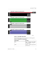
Страница 19: ...tiLINX Cable is shipped with four sets of flying lead wires A USB Cable and RS 232 Cable with adapter are also supplied For detailed information on the MultiLINX Flying Wires supported modes refer to the MutliLINX Cable chapter The following figure shows the MultiLINX Cable hardware and flying lead connection wires Table 1 2 Cable Baud Rates Cable PC Workstation MultiLINX Cable USB 1M 12M Currentl...

Страница 20: ... DONE DIN PROG INIT RST D0 D1 D3 D4 D5 D6 D7 D2 CS0 CS CS1 CS2 CLK2 OUT WS RS RDWR RDY BUSY CLK2 IN TM STATUS PWR GND CCLK DONE D P DIN PROG INIT RST RT RD TDO TRIG TDI TCK TMS CLK1 IN CLK1 OUT CS0 CS CS1 CS2 CLK2 IN CLK2 OUT WS RS RDWR RDY BUSY D0 D1 D2 D3 D4 D5 D6 D7 MultiLINX Flying Lead Connector Set 1 TM MultiLINX Flying Lead Connector Set 2 TM MultiLINX Flying Lead Connector Set 3 TM MultiLI...

Страница 21: ... to the VCC red wire and Ground black wire lines of the circuit board that is powering the Xilinx device The external power for the MultiLINX Cable is shown in the following figure R TM USB UNIVERSAL SERIAL BUS Model DLC6 Power 2 5V 0 8A to 5V 0 4A Typ Serial UC 000074 Made in U S A RS 232 CAUTION SENSITIVE ELECTRONIC DEVICE C E R RT RT TDO TRIG TDI TCK TMS CLK1 IN CLK2 OUT 2 1 4 3 PWR GND CCLK DO...

Страница 22: ...t board power is off Parallel Cable III The Parallel Cable III is a cable assembly which contains a buffer to protect your PC s parallel port and a set of headers to connect to your target system The cable can be used with a single CPLD or FPGA device or several devices connected in a daisy chain D0 D1 D2 D3 D4 D5 D6 D7 RDY BUSY CS2 CS1 CS0 CS WS GND CCLK DIN RT TDI TCK TMS RST TRIG RD TDO PWR RS ...

Страница 23: ...f flying leads one for FPGAs and one for CPLDs The CPLD leads are labelled JTAG and the FPGA leads are labelled FPGA Each flying lead has a 9 pin 6 signals 3 keys header connector on one end This connector fits onto one of the two cable headers These header connectors are keyed to assure proper orientation to the cable assembly On the other end of each flying lead are six individual wires with fem...

Страница 24: ...le III and FPGA Flying Leads The following figure shows top and bottom views of the Parallel Cable III including the FPGA and JTAG CPLD headers PROG GND FPGA Flying Lead Connector Connections to Target System DB25 Plug Connector Parallel Cable III X8325 FPGA VCC CCLK D P DIN ...

Страница 25: ...g the CPLD flying leads for configuration make sure to use the JTAG header The following figure shows the connec tions between the Parallel Cable III CPLD flying leads and a target system Parallel Cable III Top View Bottom View JTAG Header Parallel Cable III CAUTION SENSITIVE ELECTRONIC DEVICE Model DLC5 Power 5V 10mA Typ Serial JT 1 2 3 4 5 VCC JTAG FPGA GND TCK TDO TDI TMS VCC Made in U S A GND ...

Страница 26: ...ctions VCC Power Supplies VCC 5 V 10 mA typically to the cable To target system VCC GND Ground Supplies ground reference to the cable To target system ground TCK Test Clock Drives the test logic for all devices on a JTAG chain Connect to system TCK pin TDO Test Data Output data from the target system is read at this pin Connect to system TDO pin JTAG Flying Lead Connector Target System X83 TMS TDI...

Страница 27: ...s of each pin see Table 3 6and Table 3 7 of the FPGA Design Demonstration Board chapter Note If you are using the Xilinx FPGA Design Demonstration Board see the Mode Switch Settings section of the FPGA Design Demon stration Board chapter for specific configuration information Connect the flying wires to XC4000 FPGAs as shown in the following figure TDI Test Data Input this signal is used to transm...

Страница 28: ...00 Device Note If you are using the Xilinx FPGA Demonstration Board see the Mode Switch Settings section of the FPGA Design Demonstration Board chapter for specific configuration information Parallel Cable III with FPGA Flying Leads Target System X8326 CCLK GND VCC DONE DIN PROG XC4000 FPGA in Slave Serial Mode VCC GND PROG CCLK D P DIN FPGA P R O G Not Used Parallel Cable III with FPGA Flying Lea...

Страница 29: ... If you have a different serial port connection you need to provide a DB 9 DB 25 adapter Flying Leads The XChecker Cable is shipped with two sets of flying lead wires The flying lead connectors have a nine position header connector on one end The other end has eight individual wires with female connectors that fit onto standard 0 025 inch square male pins You need appropriate pins on the target sy...

Страница 30: ...s of the XChecker Cable Connection to Host Computer XChecker Cable Flying Lead Connector 1 Header 1 Header 2 Flying Lead Connector 2 DB25 Adapter DB9 Socket Connector 5V Test Fixture Enlarged to show plugs Connections to Target System Connections to Target System GND X8322 VCC GND CCLK D P DIN PROG INIT RST TRIG RD RT TDI TCK TMS CLK1 CLK0 ...

Страница 31: ...e III is grey The flying lead wires are keyed to fit into the appropriate cable header Use Header 1 for FPGAs and Header 2 for CPLDs XChecker Cable Top View Bottom View Header 2 Header 1 Model DLC4 CAUTION SENSITIVE ELECTRONIC DEVICE Power 5V 100mA Typ Serial DL 1 2 3 4 5 RT RD TRIG TDI TCK TMS CLKI CLKO VCC Made in U S A GND CCLK D P DIN PROG INIT RST X7249 ...

Страница 32: ...DI TCK TMS and RD TDO pins are connected Note TRST is an optional pin in the JTAG IEEE 1149 1 specification and is not used by XC9500 CPLDs If any of your non Xilinx parts have a TRST pin the pin should be connected to VCC Once installed properly the connectors provide power to the cable and allow download and readback of configuration data The following table describes the CPLD pin connections to...

Страница 33: ...DI Test Data In this signal is used to transmit serial test instructions and data Connect to system TDI pin TCK Test Clock this clock drives the test logic for all devices on boundary scan chain Connect to system TCK pin TMS Test Mode Select this signal is decoded by the TAP controller to control test operations Connect to system TMS pin CLKI Not used Unconnected CLKO Not used Unconnected CCLK Not...

Страница 34: ...cker Connections to XC4000 Device To configure XC3000 FPGAs the PROG wire is not used This is shown in the following figure In both cases the FPGA must be in the Serial Slave Mode Figure 1 12 XChecker Connections to XC3000 Device Pin Connection Considerations The following adjustments will make the process of connecting and downloading easier XChecker with Header 1 Target System X8323 CCLK GND VCC...

Страница 35: ...ire to the corresponding signal on the target board Next connect VCC to the 5 V on the target board 4 Connect the appropriate pins for device configuration 5 Power up the target system Cable protection ensures that the host system port cannot be damaged through normal cable operation For increased safety please check that the power to the host computer is on before the target system is powered up ...

Страница 36: ...ate See Table 1 4 If you are using the JTAG Programmer software select the cable manually as follows Output Cable Auto Connect Select your cable type then click OK Download Cable Schematic The following figure is an internal schematic of the Parallel Cable III You must use the recommended lengths for parallel cables Xilinx cables are typically six feet approximately two meters in length between th...

Страница 37: ... 100 100 100pF 100pF 100pF 100pF 5 1K 1K 01uF 1N5817 X7557 JTAG Header DB25 MALE CONNECTOR FPGA Header 100 300 300 300 300 300 DONE PROG DIN TMS_IN CTRL CLK GND GND D6 BUSY PE SHIELD 15 13 U1 14 7 3 2 5 12 9 1 6 4 11 13 8 10 U1 U1 U1 U1 6 2 4 5 3 20 25 8 11 12 U2 U2 U2 U1 74HC125 U2 74HC125 Serial JT 05000 and above for EPP parallel ports 100 U2 1 1N5817 U2 14 7 2 6 5 8 4 9 10 12 11 13 3 ...

Страница 38: ...Hardware User Guide 1 24 Xilinx Development System ...

Страница 39: ...e This chapter contains the following sections Additional MultiLINX Documentation MultiLINX Platform Support MultiLINX Flying Wires Device Configuration Modes Additional MultiLINX Documentation You can access the following mentioned application note with descriptions of device specific design techniques and approaches from the support page at http support xilinx com support searchtd htm The Gettin...

Страница 40: ...n 98 Win NT 4 0 Solaris 2 6 HP 10 2 MultiLINX Flying Wires The MultiLINX Cable is shipped with four sets of flying lead wires The following figure shows these four sets of MultiLINX flying lead connectors Table 2 1 MultiLINX Support Supported Platforms USB RS 232 Win 95 X Win 98 X X Win NT 4 0 X Solaris 2 6 X HP 10 2 X X indicates applicable ports that can be used with the MultiLINX Cable on spec ...

Страница 41: ... Works at multiple voltages 5V 3 3V and 2 5V GND Ground Supplies ground refer ence to cable PWR GND CCLK DONE D P DIN PROG INIT RST RT RD TDO TRIG TDI TCK TMS CLK1 IN CLK1 OUT CS0 CS CS1 CS2 CLK2 IN CLK2 OUT WS RS RDWR RDY BUSY D0 D1 D2 D3 D4 D5 D6 D7 MultiLINX Flying Lead Connector Set 1 TM MultiLINX Flying Lead Connector Set 2 TM MultiLINX Flying Lead Connector Set 3 TM MultiLINX Flying Lead Con...

Страница 42: ...me pin initiates a reconfiguration and indicates that the configura tion process is complete on XC3000 FPGAs DIN Data In Provides configuration data to target system during configuration and is tristated at all other times PROG Program A Low indicates the device is clearing its configura tion memory Active Low signal to initiate the configuration process INIT Initialize Initialization sequencing p...

Страница 43: ...C5200 devices RT Read Trigger Pin used to initiate a readback of target FPGA MultiLINX output Hardware Debugger provides Low to High transition on RT to initiate readback RD TDO Read Data MultiLINX input Hardware Debugger receives the readback data through the RD pin after readback is initiated Pin used to initiate a readback of target FPGA TDO is for JTAG TRIG System Trigger MultiLINX input High ...

Страница 44: ...system clock CLK1 OUT Clock Output Drives target system clock Clock can come from either the CLKI IN pin or it can be inter nally generated by the Multi LINX Cable when CLKI IN is unconnected D0 D7 Data Bus This pin is used for Virtex SelectMAP Mode An 8 bit data bus supporting the SelectMAP and Express configu ration modes CS0 CS Chip Select CS on the Virtex and CS0 on the XC4000 and XC5200 FPGAs...

Страница 45: ...Connect this pin to target system clock to synchronize the read back trigger with target system clock CLK2 OUT Clock Output Drives target system clock Clock can come from either the CLK2 IN pin or it can be inter nally generated by the Multi LINX Cable when CLK2 IN is unconnected WS Write Select The WS pin repre sents Write Select control for the Asynchronous Peripheral config uration mode on XC40...

Страница 46: ...g Wire Set 1 are connected to the VCC red wire and Ground black wire lines of the circuit board that is powering the Xilinx device The minimum input voltage to the cable is 2 5 V 8 A The maximum input voltage is 5 V 4 A External Power for the MultiLINX Cable An optional method of powering the MultiLINX Cable is to use an external DC power supply not supplied as shown in the following RS RDWR Read ...

Страница 47: ...an external power supply make sure that the ground of the supply the MultiLINX Cable and the circuit board are all tied together An advantage of the external DC power supply is that no power is taken away from the circuit board and the MultiLINX Cable D0 D1 D2 D3 D4 D5 D6 D7 RDY BUSY CS2 CS1 CS0 CS WS GND CCLK DIN RT TDI TCK TMS RST TRIG RD TDO PWR RS RDWR CLK2 IN CLK2 OUT CLK1 IN CLK1 OUT DONE D ...

Страница 48: ...ollowing table Downloading Configuration Data This section details the connections needed to download configura tion data with the MultiLINX Cable Slave Serial Mode XC3000 The following figure shows in detail the Slave Serial Mode connec tions to a XC3000 device for Downloading Configuration Data Table 2 3 MultiLINX Device Configuration Modes Configuration Mode Device Virtex Spartan XC9500 XC5200 ...

Страница 49: ...onnec tions for Virtex Spartan XC5200 and XC4000 devices D0 D1 D2 D3 D4 D5 D6 D7 RDY BUSY CS2 CS1 CS0 CS WS GND CCLK DIN RT TDI TCK TMS RST TRIG RD TDO PWR VCC RS RDWR CLK2 IN CLK2 OUT CLK1 IN CLK1 OUT DONE D P PROG INIT 4 2 3 1 NOTE Pull up resistors are 4 7k ohm VCC Circuit Board XILINX device MultiLINX Connectors M0 M1 M2 INIT CCLK RESET PWRDN DIN D P VCC VCC VCC VCC VCC VCC X8942 ...

Страница 50: ...tiLINX Cable SelectMAP Mode Virtex The following figure shows in detail the SelectMAP Mode connec tions for Virtex devices D0 D1 D2 D3 D4 D5 D6 D7 RDY BUSY CS2 CS1 CS0 CS WS GND CCLK DIN RT TDI TCK TMS RST TRIG RD TDO PWR VCC VCC RS RDWR CLK2 IN CLK2 OUT CLK1 IN CLK1 OUT DONE D P PROG INIT 4 2 3 1 NOTE Pull up resistors are 4 7k ohm VCC Circuit Board XILINX device MultiLINX Connectors VCC VCC VCC ...

Страница 51: ... The following figure shows in detail the JTAG Mode connections for XC9000 Virtex Spartan XC5200 and XC4000 devices D0 D1 D2 D3 D4 D5 D6 D7 RDY BUSY CS2 CS1 CS0 CS WS GND CCLK DIN RT TDI TCK TMS RST TRIG RD TDO PWR Vcco RS RDWR CLK2 IN CLK2 OUT CLK1 IN CLK1 OUT DONE D P PROG INIT 4 2 3 1 NOTE Pull up resistors are 4 7k ohm Circuit Board XILINX device MultiLINX Connectors VCC VCC Vcco Vcco M0 M1 M2...

Страница 52: ...e Serial Mode XC3000 The following figure shows in detail the Slave Serial Mode connec tions for the XC3000 device D0 D1 D2 D3 D4 D5 D6 D7 RDY BUSY CS2 CS1 CS0 CS WS GND CCLK DIN RT TDI TCK TMS RST TRIG RD TDO PWR VCC RS RDWR CLK2 IN CLK2 OUT CLK1 IN CLK1 OUT DONE D P PROG INIT 4 2 3 1 NOTE Pull up resistors are 4 7k ohm Circuit Board XILINX device MultiLINX Connectors see data sheet of the device...

Страница 53: ...D2 D3 D4 D5 D6 D7 RDY BUSY CS2 CS1 CS0 CS WS GND CCLK DIN RT TDI TCK TMS RST TRIG RD TDO PWR VCC RS RDWR CLK2 IN CLK2 OUT CLK1 IN CLK1 OUT DONE D P PROG INIT 4 2 3 1 NOTE Pull up resistors are 4 7k ohm VCC Circuit Board XILINX device MultiLINX Connectors VCC VCC VCC VCC VCC VCC System Clock x System Clock y optional M0 RTRIG M1 RDATA M2 INIT CCLK RESET DIN D P PWRDN User I O TRIGGER GCK x GCK y op...

Страница 54: ...D2 D3 D4 D5 D6 D7 RDY BUSY CS2 CS1 CS0 CS WS GND CCLK DIN RT TDI TCK TMS RST TRIG RD TDO PWR VCC RS RDWR CLK2 IN CLK2 OUT CLK1 IN CLK1 OUT DONE D P PROG INIT 4 2 3 1 NOTE Pull up resistors are 4 7k ohm VCC Circuit Board XILINX device MultiLINX Connectors VCC System Clock x System Clock y optional optional only used for probing VCC VCC VCC VCC M0 M1 M2 INIT CCLK RESET DIN DONE User I O TRIGGER GCK ...

Страница 55: ...D0 D1 D2 D3 D4 D5 D6 D7 RDY BUSY CS2 CS1 CS0 CS WS GND CCLK DIN RT TDI TCK TMS RST TRIG RD TDO PWR Vcco RS RDWR CLK2 IN CLK2 OUT CLK1 IN CLK1 OUT DONE D P PROG INIT 4 2 3 1 NOTE Pull up resistors are 4 7k ohm Circuit Board XILINX device MultiLINX Connectors VCC VCC Vcco Vcco User I O TRIGGER optional System Clock x System Clock y optional M0 M1 M2 CCLK CS DONE PROG INIT D7 D6 D5 D3 D4 D2 D1 D0 WRI...

Страница 56: ...1 CS0 CS WS GND CCLK DIN RT TDI TCK TMS RST TRIG RD TDO PWR Vcco RS RDWR CLK2 IN CLK2 OUT CLK1 IN CLK1 OUT DONE D P PROG INIT 4 2 3 1 NOTE Pull up resistors are 4 7k ohm Circuit Board XILINX device MultiLINX Connectors VCC VCC Vcco Vcco optional System Clock x System Clock y optional M0 M1 M2 CCLK CS DONE PROGRAM INIT D7 D6 D5 D3 D4 D2 D1 D0 WRITE BUSY DOUT GCK x GCK y User Logic flip flops latche...

Страница 57: ...onnections for verification of configuration data only with Spartan XC5200 and XC4000 devices D0 D1 D2 D3 D4 D5 D6 D7 RDY BUSY CS2 CS1 CS0 CS WS GND CCLK DIN RT TDI TCK TMS RST TRIG RD TDO PWR VCC RS RDWR CLK2 IN CLK2 OUT CLK1 IN CLK1 OUT DONE D P PROG INIT 4 2 3 1 NOTE Pull up resistors are 4 7k ohm Circuit Board XILINX device MultiLINX Connectors see data sheet of the device if applicable only X...

Страница 58: ...s in detail the connections for verification of configuration data only with the XC3000 device D0 D1 D2 D3 D4 D5 D6 D7 RDY BUSY CS2 CS1 CS0 CS WS GND CCLK DIN RT TDI TCK TMS RST TRIG RD TDO PWR VCC RS RDWR CLK2 IN CLK2 OUT CLK1 IN CLK1 OUT DONE D P PROG INIT 4 2 3 1 Circuit Board XILINX device MultiLINX Connectors optional only used for probing CCLK User I O TRIGGER User I O RD User I O RT X8933 ...

Страница 59: ...Mode XC3000 The following figure shows in detail the Slave Serial Mode connec tions for synchronous probing using the XC3000 device D0 D1 D2 D3 D4 D5 D6 D7 RDY BUSY CS2 CS1 CS0 CS WS GND CCLK DIN RT TDI TCK TMS RST TRIG RD TDO PWR VCC RS RDWR CLK2 IN CLK2 OUT CLK1 IN CLK1 OUT DONE D P PROG INIT 4 2 3 1 Circuit Board XILINX device MultiLINX Connectors optional only used for probing M0 RTRIG M1 RDAT...

Страница 60: ...l Mode connec tions for synchronous probing using Spartan XC5200 and XC4000 devices D0 D1 D2 D3 D4 D5 D6 D7 RDY BUSY CS2 CS1 CS0 CS WS GND CCLK DIN RT TDI TCK TMS RST TRIG RD TDO PWR VCC RS RDWR CLK2 IN CLK2 OUT CLK1 IN CLK1 OUT DONE D P PROG INIT 4 2 3 1 Circuit Board XILINX device MultiLINX Connectors optional only used for probing M0 RTRIG M1 RDATA CCLK User I O TRIGGER X8932 ...

Страница 61: ...D4 D5 D6 D7 RDY BUSY CS2 CS1 CS0 CS WS GND CCLK DIN RT TDI TCK TMS RST TRIG RD TDO PWR VCC RS RDWR CLK2 IN CLK2 OUT CLK1 IN CLK1 OUT DONE D P PROG INIT 4 2 3 1 NOTE Pull up resistors are 4 7k ohm Circuit Board XILINX device MultiLINX Connectors System Clock x System Clock y optional GCK x optional VCC VCC VCC VCC VCC VCC VCC GCK y CCLK DIN DONE RESET INIT M0 M1 M2 VCC TCK User I O TRIGGER User I O...

Страница 62: ...cco RS RDWR CLK2 IN CLK2 OUT CLK1 IN CLK1 OUT DONE D P PROG INIT 4 2 3 1 NOTE Pull up resistors are 4 7k ohm Circuit Board XILINX device MultiLINX Connectors VCC VCC Vcco Vcco optional System Clock x User I O TRIGGER User I O System Clock y optional M0 M1 M2 CCLK CS DONE PROGRAM INIT D7 D6 D5 D3 D4 D2 D1 D0 WRITE BUSY DOUT GCK x GCK y User Logic flip flops latches LUTRAMS block RAMS Capture Contro...

Страница 63: ...milies and the Xilinx software development system This chapter contains the following sections Demonstration Board Overview General Components XC4003E Components XC3020A Components Mode Switch Settings Demonstration Board Operation Demonstration Board Overview The following sections detail the device and software support for the FPGA Demonstration Board as well as describing the board s general fe...

Страница 64: ...oftware Support Two Xilinx software packages can be used with this demonstration board XChecker is a command line text only program available for both PC and Workstation platforms The XChecker Software supports the XChecker Cable only Hardware Debugger a GUI type program is the recommended software for use with this demonstration board For more infor mation on using Hardware Debugger with the demo...

Страница 65: ...s to provide logic inputs to the FPGAs Program Reset and Spare Active Low push button switches which are common to both FPGAs An XC3000A display for the XC3000 device The display uses eight LED bars in one row and one 7 segment LED as shown in the following figure An XC4000A display for the XC4000 device The display uses eight LED bars in one row and two 7 segment LEDs as shown in the following fi...

Страница 66: ...1 FPGA Demonstration Board Displays General Components This section describes the common components that are found on the FPGA Demonstration Board The following figure shows the compo nent layout of the FPGA Demonstration Board U6 U7 U8 XC3000 XC4000 X4710 XC3000 XC4000 7 Segment Display Bars ...

Страница 67: ...DEMO BOARD XC4003E PC84 XC3020A PC68 RN4 RN3 GND R5 C5 C6 SW3 59 60 R4 R1 R2 44 43 27 28 C8 C7 D17 ASSY 0430822 RESET SW4 SPARE SW5 PROG SW6 Y1 26 C4 11 10 1 2 3 4 5 6 7 8 RN9 C9 LO HI RN13 RN10 RN11 RN14 RN15 RN16 RN18 RN19 RN17 D1 D9 RN12 U2 U3 C2 U1 U4 J1 J3 J5 C1 RN1 SW1 RN5 RN6 RN7 M0 M1 M2 INP MPE SPE MCLK DOUT M1 M2 RST MPE SPE M0 INIT C3 RN2 SW2 PWR 11 33 53 54 73 J2 J12 J10 J7 D8 D16 J9 5...

Страница 68: ...to connect the unregulated power source The hole with the square pad marked with a is the positive input The other hole marked with a is circuit ground The positive input is connected through the power on off switch SW2 1 to U3 1 which is the optional 5 V regulator U3 must be installed to use this input 5 V Regulator Option U3 You can install a three terminal 5 V regulator such as the LM2940CT sho...

Страница 69: ...oint triangles the trace cut option for the XC3020A is under its socket and the trace cut option for the XC4003E is under R3 The SPARE signal is pulled High through a 27 kilohm resistor PROG Pushbutton SW6 The PROG pushbutton applies an active Low signal to the DONE PROGRAM input on the XC3020A FPGA socket at pin 45 and to the PROGRAM input on the XC4003E FPGA socket at pin 55 The PROG signal is n...

Страница 70: ...olates it from the switch so it is possible to define the pins as outputs You can also drive the pins from an external source by connecting that signal to the FPGA probe point header The following table lists the FPGA pin connections Table 3 2 Input Switch Pin Connections Switch XC3020A XC4003E SW3 1 11 19 SW3 2 13 20 SW3 3 15 23 SW3 4 17 24 SW3 5 19 25 SW3 6 21 26 SW3 7 23 27 SW3 8 24 28 X4744 1K...

Страница 71: ... be on while the FPGA is in its internal clearing state then it should remain off during configuration If the decimal point comes back on a programming error has occurred The decimal points on U6 and U7 are tied to the Low During Config uration LDC pins of the XC3020A and XC4003E respectively The decimal points are on while the FPGAs wait to be configured The following table shows the I O pin defi...

Страница 72: ... and D9 through D16 connect to the XC4003E You can turn on an LED by driving its corresponding FPGA pin Low with a logic 0 The following table shows the pin connections for the LED indicators Table 3 4 LED Indicators for XC3020A and XC4003E LED XC3020A Pin LED XC4003E Pin D1 37 D9 61 D2 36 D10 62 D3 41 D11 65 D4 33 D12 66 D5 32 D13 57 D6 31 D14 58 D7 28 D15 59 D8 29 D16 60 X4709 a g e c d b f Deci...

Страница 73: ...mon stration Board The oscillator output drives the XC3020A XTL2 input at pin 43 and the XC4003E PGCK1 input at pin 13 Prototype Area The Prototype area is a 0 1 inch grid of holes where you can add additional circuitry to the demonstration board A 5 V bus compo Table 3 5 I O Line Connections for XC3020A and XC4003E Devices I O Line XC3020A Pin XC4003E Pin 0 61 10 1 62 9 2 63 8 3 64 7 4 65 6 5 66 ...

Страница 74: ...us solder side are available on the perim eter of this area There are also locations for filter capacitors XC4003E Components This section describes the components on the FPGA Demonstration Board which are used with the XC4003E device The following sche matic shows this device ...

Страница 75: ...CE 4 CLK 2 OE R 3 U2 1765 7 1 0 RST 1 6 1 5 5 27K 1 2 1 7 1 8 1 4 1 9 1 3 9 11 13 15 17 7 J2A 1 2 J7 CUT OPTION 1 2 560 3 4 7 8 5 6 3 4 5 6 7 8 1 2 560 1 2 560 3 4 7 8 1 2 560 3 4 5 6 5 6 7 8 2 15 MPE 3 14 SPE R3 100K 8 9 INIT D17 MBR030 8 7 3 6 4 2 1 9 1 0 5 5 U7 HPSP5551 SW4 RESET SW6 PROG SW5 SPARE 8 7 3 6 4 2 1 9 1 0 5 U8 U1 U2 U3 U4 U5 7 8 5 GND 3 18 52 2 11 33 42 54 63 74 5 2 1 35 1 12 21 31...

Страница 76: ...urned on and SPE turned off the configuration PROM U2 is reset by the RESET pushbutton SW4 Configuration mode must be set to master serial After a Reset or powerup the first bitstream stored in the serial PROM is loaded into the XC4003E Pressing RESET resets the serial PROM address pointer Pressing PROG SW6 loads the XC4003E with the first bitstream again If you press PROG without pressing RESET t...

Страница 77: ... 56 INIT Initialize SW2 8 When this switch is on it connects the XC3020A INIT pin to the XC4003E INIT pin This connection is used to configure FPGAs in a daisy chain with the XC4003E at the head of the chain Note INIT should only be used to configure FPGAs in a daisy chain XChecker Parallel Cable III Connector J2 The following table provides a detailed description of the J2 XChecker Parallel Cable...

Страница 78: ...configuration is complete Connects to XC4003E output pin 53 J2 10 TDI Inputs boundary scan data to the XC4003E Connects to XC4003E pin 15 J2 11a DIN Provides configura tion data during configuration Connects to XC4003E DIN input pin 71 J2 12 TCK Input boundary scan clock to the XC4003E Connects to pin 16 J2 13a PROG Provides program pulse causing the FPGA to configure Connects to XC4003E PROG inpu...

Страница 79: ...igures the XC4003E or the XC4003E and XC3020A connected in a daisy chain The configuration mode must be in the master serial mode to configure from the serial PROM J2 15 INIT Goes Low if CRC error occurs during configuration Connects to XC4003E INIT pin 41 J2 16 CLK1 A system clock input to XChecker Cable to be controlled and output on CLK0 Connects to tiepoint J10 2 J2 17 RST Connects to jumper J...

Страница 80: ... XTL1 47 I O 48 I O 49 I O 50 I O 51 I O 53 I O 54 I O 55 I O 56 I O 57 DIN 58 DOUT 59 CCLK 60 U4 XC3020A INP3 5 6 3 4 1 2 1K 7 8 5 6 3 4 1 2 1K 1 2 4 7K 1 4 1 3 1 5 1 6 1 7 1 8 1 9 CUT R2 100K 1 3 R1 100K 1 3 9 11 13 15 17 7 J1A 5 1 2 J5 R7 27K 8 9 DOUT 7 10 MCLK 2 15 MPE DATA 1 CEO 6 CE 4 CLK 2 OE R 3 U1 1765 3 14 SPE OPTION C6 0 1uF C5 5 0 1uF R6 100K 1 16 PWR 1 2 J12 1 2 J9 VIN 1 VOUT 3 5 U3 5...

Страница 81: ...through 84 respectively The XC3020A pins share the XC4003E probe points header XC3020A Configuration Switches SW1 The following sections describe each of the SW1 switches For more information on configuring the XC3020A device see the Mode Switch Settings section INP Input Switch SW1 1 INP is an extra switch which you can connect to provide an extra logic input to the XC3020A pin 46 and the XC4003E...

Страница 82: ...tream stored in the serial PROM The number of bitstreams that can be sequentially loaded is limited by the size of the serial PROM SPE Single Program Enable SW1 3 When SPE is on and MPE is off the configuration PROM U1 is reset by the XC3020A s INIT output which is driven Low whenever you press PROG SW6 The first bitstream stored in the serial PROM is loaded into the XC3020A FPGA Note MPE and SPE ...

Страница 83: ...2 to the data in line of the XC3020A This connection configures FPGAs in a daisy chain with the XC4003E at the head Note MCLK and DOUT should only be used to configure the FPGAs in a daisy chain XChecker Parallel Cable III Connector J1 The following table describes the pins and functions of the XChecker Parallel Cable III J1 connector Table 3 7 XChecker Parallel Cable III Connector J1 Pin Name Fun...

Страница 84: ... J1 7a CCLK Provides clock during configura tion or readback Connects to XC3020A input pin 50 J1 8 N C b J1 9a D P Starts configuration and indicates completion Connects to XC3020A DONE PROGRAM pin 45 J1 10 N C b J1 11a DIN Provides configura tion data during configuration Connects to XC3020A DIN input pin 58 J1 12 N C b J1 13 N C b J1 14 N C b Table 3 7 XChecker Parallel Cable III Connector J1 Pi...

Страница 85: ...ion Oscillator Components R1 C5 R2 C6 R1 C5 and R2 C6 are two RC networks that connect to the XC3020A at pins 12 and 14 These RC networks are for use in a relaxation oscil lator such as the circuit is shown in the following figure J1 15 N C bb J1 16 CLKI System clock input to XChecker Cable to be controlled and output on CLKO Connects to tiepoint J3 2 J1 17 RST Connects to jumper J5 If connected a...

Страница 86: ... 1uF the oscillator generates an output frequency of approximately 100 Hz The following figure shows the RC Network waveforms Figure 3 10 RC Network Waveforms The formula for calculating the RC network is as follows T T1 T2 N R1C5 R2C6 where X6127 R1 Vcc R2 C5 C6 nameQ name set name reset nameQL CQ OBUFT IBUF IBUF OBUFT CQL X4715 T T2 T1 VT VT Q C5 C6 ...

Страница 87: ...I From the serial PROM single program From the serial PROM multiple program In a daisy chain The following table lists the names and positions of the SW1 and SW2 switches for configuring the XC3020A FPGA from the XChecker or Parallel Cable III Table 3 8 Configuring the XC3020A from the XChecker Parallel Cable III Switch Name Position Switch Name Position SW1 1 INP X SW2 1 PWR X SW1 2 MPE OFF SW2 2...

Страница 88: ...input The following table lists the names and positions of the SW1 and SW2 switches for configuring the XC3020A FPGA from the serial PROM Table 3 9 Configuring the XC4003E from the XChecker Parallel Cable III Switch Name Position Switch Name Position SW1 1 INP X SW2 1 PWR X SW1 2 MPE X SW2 2 MPE OFF SW1 3 SPE X SW2 3 SPE OFF SW1 4 M0 X SW2 4 M0 ON SW1 5 M1 X SW2 5 M1 ON SW1 6 M2 X SW2 6 M2 ON SW1 ...

Страница 89: ...from the Serial PROM Single Program Switch Name Position Switch Name Position SW1 1 INP X SW2 1 PWR X SW1 2 MPE X SW2 2 MPE OFF SW1 3 SPE X SW2 3 SPE ON SW1 4 M0 X SW2 4 M0 OFF SW1 5 M1 X SW2 5 M1 OFF SW1 6 M2 X SW2 6 M2 OFF SW1 7 MCLK OFF SW2 7 RST X SW1 8 DOUT OFF SW2 8 INIT OFF X indicates don t care Table 3 12 Configuring the XC3020A from the Serial PROM Multiple Program Switch Name Position S...

Страница 90: ...e Table 3 13 Configuring the XC4003E from the Serial PROM Multiple Program Switch Name Position Switch Name Position SW1 1 INP X SW2 1 PWR X SW1 2 MPE X SW2 2 MPE ON SW1 3 SPE X SW2 3 SPE OFF SW1 4 M0 X SW2 4 M0 OFF SW1 5 M1 X SW2 5 M1 OFF SW1 6 M2 X SW2 6 M2 OFF SW1 7 MCLK OFF SW2 7 RST X SW1 8 DOUT OFF SW2 8 INIT OFF X indicates don t care Table 3 14 Configuring the XC3020A and XC4003E in a Dais...

Страница 91: ...2 8 INIT ON X indicates don t care Table 3 15 Configuring the XC3020A and XC4003E in a Daisy Chain from the Serial PROM Single Program Switch Name Position Switch Name Position SW1 1 INP X SW2 1 PWR X SW1 2 MPE OFF SW2 2 MPE OFF SW1 3 SPE OFF SW2 3 SPE ON SW1 4 M0 ON SW2 4 M0 OFF SW1 5 M1 ON SW2 5 M1 OFF SW1 6 M2 ON SW2 6 M2 OFF SW1 7 MCLK ON SW2 7 RST X SW1 8 DOUT ON SW2 8 INIT ON X indicates don...

Страница 92: ...003E FPGA Note The Parallel Cable III can also be used for FPGA configuration For Parallel Cable III connection information refer to the External Power for the MultiLINX Cable section of the Cable Hardware chapter Demonstration Designs Demonstration designs are supplied with Xilinx Foundation and Alliance Series software You can view or edit the demonstration designs Before editing you must compil...

Страница 93: ...nclude the Startup symbol in your design and select the location of the RESET pin Attach pin 56 to an inverter and the GSR pin on the Startup symbol GSR is active High so you must include an inverter between the pad and the Startup symbol 2 Generate a bitstream for the design design_name bit with the appropriate configuration options using the BitGen program 3 Optionally create a PROM File 4 Gener...

Страница 94: ... edit the demonstration designs supplied with the Xilinx software tools Note Make backups before making changes to any demonstration design files 1 Place and route the design Produce a routed design design_name using a design entry tool and the appropriate place and route tool 2 Generate a configuration bitstream for the design design_name bit with the appropriate configuration options using the B...

Страница 95: ...a tion switches apply power to the FPGA Demonstration Board This step configures the FPGA when the DONE pin goes High it indicates that the design logic is active 8 Start your configuration software For information on starting the Hardware Debugger software see the following section Starting Hardware Debugger The following section includes a checklist for opening the Hardware Debugger software For...

Страница 96: ... Web site and on the AppLINX CD The Web site location is http support xilinx com support techsup tutorials index htm Please contact your local Sales Repre sentative for a copy of the AppLINX CD Calculator tutorial designs for Mentor and Cadence are available on the Xilinx CAE Interface CD ROM at the following locations Mentor Tutorial on a Workstation CD DRIVE or server mentor tutorial calc_4ke ca...

Страница 97: ...tails the features and support for the CPLD Demonstration Board The demonstration board uses a surface mounted 555 timer with resistor and capacitor values set for 14 Hz operation This oscillator clocks a simple test design a Johnson counter implemented in the XC9536 this counter drives LEDs used to verify operation Software and Download Cable Support The CPLD Demonstration Board is shipped with t...

Страница 98: ... area has 299 holes 13 columns x 23 rows for attaching additional circuitry The holes are 0 038 inch diameter on 0 10 inch centers Two pairs of these holes are connected to 5V and GND along the left side of the prototyping area Power Supply The Demonstration Board allows the attachment of an external regu lated 5V power supply via the pads at J2 If a 5V regulator is installed at location U2 with a...

Страница 99: ...nto a SERPAC plastic case Model H 65 AC This case can be purchased from SERPAC 619 Commer cial Ave Covina CA 91723 Tel 818 331 0517 Fax 818 331 8584 http www serpac com Demonstration Board Schematics A schematic of this demonstration board is shown in the following figure 1 5V 1A low dropout reg U2 LM2940CT 5 0 1 22uf 16V Tantalum cap C4 P2040 Table 4 1 Digi Key Parts List Quantity Descriptions Re...

Страница 100: ...D5 D6 D7 D8 R1 R2 R3 R4 R5 R6 R7 R8 470 470 470 470 470 470 470 470 I O I O I O I O I O GND I O VCC I O I O I O GTS2 VCC GTS1 I O I O I O I O I O I O GCK1 GCK2 GSR I O I O I O I O I O I O VCC GND TDO I O GCK3 I O I O I O GND I O I O I O TDI TMS TCK VCC GND TCK TDO TDI TMS C4 22uF U2 LM2940 9V J3 9V BATTERY 60mA 2 3 4 5 7 9 10 6 8 1 11 C3 047uF U1 XC9536 ON SW1 OFF GND TRIG VCC OUT CONT RESET DISCH...

Страница 101: ...nter tutorial which includes the following five design entry methods JCT_SCH schematic only JCT_ABL ABEL only JCT_SABL schematic with ABEL macro JCT_VHD VHDL only JCT_SVHD schematic with VHDL macro Example I Schematic Design Entry Example 1 shows the readme txt file that is located in the project directories of the Jcounter tutorial designs in the Xilinx Foundation R R ISP DEMO BOARD 1 2 11 10 9 8...

Страница 102: ... with XVHDL macro JCOUNTER VHD TARGET DEVICE XC9536 VQ44 any speed I O Pins CLK input free running clock Q0 Q7 counter outputs OPERATION The counter is triggered on rising edge of the clock CLK The following is the sequence of states on outputs Q Q7 Q0 00000000 00000001 00000011 00000111 00001111 00011111 00111111 01111111 11111110 11111110 11111100 11111000 11110000 11100000 11000000 10000000 000...

Страница 103: ...sign Flow tutorial in the Foundation Series On Line Help System DEMO BOARD The JEDEC programming file produced by this project can be downloaded into the CPLD Demo Board HW CPLD DEMOBD Example 2 VHDL Design Entry Example 2 shows the same design done in VHDL while using Xilinx Foundation software library IEEE use IEEE std_logic_1164 all library metamor use metamor attributes all entity jcounter is ...

Страница 104: ...pinnum of Dout signal is p13 14 16 18 19 20 21 22 end jcounter architecture jcounter_arch of jcounter is begin if CLK event and CLK 1 then CLK rising edge Dout 7 downto 1 Dout 6 downto 0 shift Dout 7 downto 1 Dout 6 downto 0 shift Dout 0 not Dout 7 Last bit inverted back into first bit end if end process end jcounter_arch ...

Страница 105: ... CPLD is an erasable programmable logic device that can be programmed with a schematic or a behavioral design Daisy Chain A daisy chain is a series of bitstream files concatenated in one file It can be used to program several FPGAs connected in a daisy chain board configuration Download Dowloading is the process of configuring or programming a device by sending bitstream data to the device FPGA Fl...

Страница 106: ...configuration mode supported by the following MultiLINX devices Virtex Spartan XC9500 XC5200 and XC4000 MultiLINX Cable The MultiLINX cable is a device for configuring and verifying Xilinx FPGAs and CPLDs MultiLINX Flying Wires The MultiLINX flying wires consist of four sets that are included with the MultiLINX Cable Parallel Cable III Parallel Cable III is a cable assembly which contains a buffer...

Страница 107: ...ported by the MultiLINX device Virtex Slave Serial Mode Slave Serial Mode is a MultiLINX configuration mode supported by the following MultiLINX devices Virtex Spartan XCS5200 and XC3000 Universal Serial Buss USB Port The USB Port is where the MultiLINX cable connects to on the host computer XChecker Cable The XChecker hardware consists of a cable assembly with internal logic a test fixture and a ...

Страница 108: ...Hardware User Guide Glossary 4 Xilinx Development System ...

Отзывы: