Hardware User Guide
3-6
Xilinx Development System
is ground. The power supply should provide at least 250 mA of
current to drive the LED displays.
Unregulated Power Input (J12)
This input provides a way to power the FPGA Demonstration Board
from an unregulated source, such as a 9 V battery or an AC adapter.
Typically, the input should be 7VDC - 12VDC at 250 mA. You must
consider the power dissipation requirements of the U3 voltage regu-
lator if the voltage input is greater than 9 V.
The J12 unregulated power input provides two holes to connect the
unregulated power source. The hole with the square pad, marked
with a "+" is the positive input. The other hole, marked with a "-" is
circuit ground. The positive input is connected through the power
on-off switch SW2–1 to U3–1, which is the op5 V regulator. U3
must be installed to use this input.
+5 V Regulator Option (U3)
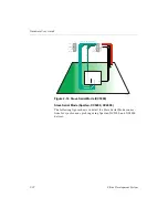
You can install a three te5 V regulator, such as the LM2940CT
shown in the following figure. This regulator powers the demonstra-
tion board from an unregulated power supply, such as a +9 V battery.
Pin 1 (square pad) is Vin, pin 2 is ground, and pin 3 is +5 V out.
Note
Insulate the metal heat sink tab of the regulator from traces and
vias on the PCB.
Figure 3-3 LM5 V Regulator
X4692
Pin1
LM2940CT
Содержание MultiLINX DLC4
Страница 2: ...Hardware User Guide ...
Страница 10: ...Hardware User Guide vi Xilinx Development System ...
Страница 38: ...Hardware User Guide 1 24 Xilinx Development System ...
Страница 108: ...Hardware User Guide Glossary 4 Xilinx Development System ...


