


W83627DHG
Publication Release Date: Aug, 22, 2007
-58- Version
1.4
(1)If SYSFANOUT is programmed for PWM output (Bank0 Index 04h,bit0 is 0)
Bit 7-0: The PWM duty cycle is equal to this eight-bit value, divided by 255, times 100%. FFh creates a
duty cycle of 100%, and 00h creates a duty cycle of 0%.
(2)If SYSFANOUT is programmed for DC Voltage output (Bank0 Index 04h,bit0 is 1)
Bit 7-2: SYSFANOUT voltage control. The output voltage is calculated according to this equation.
OUTPUT Voltage =
64
*
FANOUT
AVCC
Bit 1-0: Reserved.
8.5 CPUFANOUT0 PWM Output Frequency Configuration Register - Index 02h
(Bank 0)
Register Location:
02h
Power on Default Value: 04h
Attribute: Read/Write
Size: 8
bits
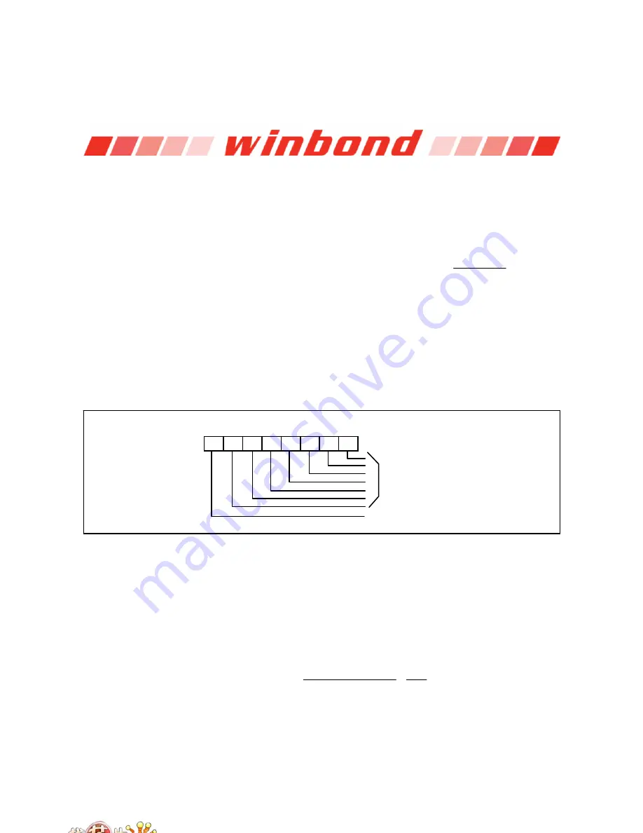
7 6 5 4 3 2 1 0
PWM_CLK_SEL2
PWM_SCALE2
The register is meaningful only when CPUFANOUT0 is programmed for PWM output.
Bit 7: CPUFANOUT0 PWM Input Clock Source Select. This bit selects the clock source for PWM
output.
0: clock source is 24 MHz.
1: clock source is 180 KHz.
Bit 6-0: CPUFANOUT0 PWM Pre-Scale divider. The clock source for PWM output is divided by this
seven-bit value to calculate the actual PWM output frequency.
PWM output frequency
=
256
1
Divider
Pre_Scale
Clock
Input
∗
The maximum value of the divider is 127 (7Fh), and it should not be set to 0.
Содержание W83627DHG
Страница 2: ......


