


29
Plasma TV Service Manual
05/01/2006
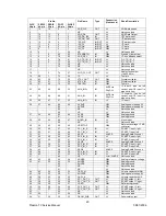
(VSB)
ADP2
M7
O
MSB
−
6 of direct analog-to-digital converted output data
(VSB)
V
DDD11
M8
P
digital supply voltage 11 (peripheral cells)
V
DDD12
M9
P
digital supply voltage 12 (core)
RTS0
M10
O
real-time status or sync information, controlled by
subaddresses 11H and 12H
V
DDD13
M11
P
digital supply voltage 13 (peripheral cells)
AMXCLK
M12
I
audio master external clock input
FSW
M13
I/pd
fast switch (blanking) with internal pull-down inserts
component inputs into CVBS signal
ICLK M14
I/O
clock output signal for image port, or optional
asynchronous back-end clock input
TEST13
N1
NC
do not connect, reserved for future extensions and for testing
TEST14
N2
I/pu
do not connect, reserved for future extensions and for testing
TEST15
N3
I/pd
do not connect, reserved for future extensions and for testing
CE
N4
I/pu
chip enable or reset input (with internal pull-up)
LLC2
N5
O
line-locked 1 ¤2 clock output (13.5 MHz nominal)
CLKEXT
N6
I
external clock input intended for analog-to-digital conversion
of VSB signals (36 MHz)
ADP5
N7
O
MSB - 3 of direct analog-to-digital converted output data
(VSB)
ADP0
N8
O
LSB of direct analog-to-digital converted output data (VSB)
SCL
N9
I
serial clock input (I 2 C-bus)
RTS1
N10
O
real-time status or sync information, controlled by
subaddresses 11H and 12H
ASCLK
N11
O
audio serial clock output
ITRDY
N12
I
target ready input for image port data
TEST16
N13
NC
do not connect, reserved for future extensions and for testing
TEST17
N14
NC
do not connect, reserved for future extensions and for testing
TEST18
P2
I/O
do not connect, reserved for future extensions and for testing
EXMCLR P3
I/pd
external mode clear (with internal pull-down)
LLC
P4
O
line-locked system clock output (27 MHz nominal)
RES
P5
O
reset output (active LOW)
ADP8
P6
O
MSB of direct analog-to-digital converted output data (VSB)
ADP4
P7
O
MSB - 4 of direct analog-to-digital converted output data
(VSB)
ADP1
P8
O
MSB - 7 of direct analog-to-digital converted output data
(VSB)
INT_A
P9
O/od
I
2
C-bus interrupt flag (LOW if any enabled status bit has
changed)
SDA
P10
I/O/od
serial data input/output (I 2 C-bus)
AMCLK
P11
O
audio master clock output, up to 50% of crystal clock
ALRCLK
P12
O/st/pd
audio left/right clock output; can be strapped to supply via a
3.3 kW resistor to indicate
that the default 24.576 MHz crystal (ALRCLK = 0; internal
pull-down) has been replaced
by a 32.110 MHz crystal (ALRCLK = 1); see notes 5 and 7
TEST19
P13
I/pu
do not connect, reserved for future extensions and for testing:
scan input
Notes
1. I = input, O = output, P = power, NC = not connected, st = strapping, pu = pull-up, pd = pull-down, od
= open-drain.
2. In accordance with the “IEEE1149.1” standard the pads TDI, TMS, TCK and TRST are input pads
with an internal pull-up transistor and TDO is a 3-state output pad.
3. For board design without boundary scan implementation connect the TRST pin to ground.
4. This pin provides easy initialization of the Boundary Scan Test (BST) circuit. TRST can be used to
force the Test Access Port (TAP) controller to the TEST_LOGIC_RESET state (normal operation) at
once.
5. Pin strapping is done by connecting the pin to the supply via a 3.3
κΩ
resistor. During the power-up
reset sequence the corresponding pins are switched to input mode to read the strapping level. For the
default setting no strapping
Содержание 17MB11
Страница 1: ...50 PLASMA TV 17MB11 SERVICE MANUAL...
Страница 50: ...47 Plasma TV Service Manual 25 08 2005 15 CIRCUIT DIAGRAMS...
Страница 51: ...48 Plasma TV Service Manual 25 08 2005...
Страница 52: ...49 Plasma TV Service Manual 25 08 2005...
Страница 53: ...50 Plasma TV Service Manual 25 08 2005...
Страница 54: ...51 Plasma TV Service Manual 25 08 2005...
Страница 55: ...52 Plasma TV Service Manual 25 08 2005...
Страница 56: ...53 Plasma TV Service Manual 25 08 2005...
Страница 57: ...54 Plasma TV Service Manual 25 08 2005...
Страница 58: ...55 Plasma TV Service Manual 25 08 2005...
Страница 59: ...56 Plasma TV Service Manual 25 08 2005...