


11
Plasma TV Service Manual
05/01/2006
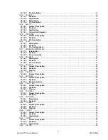
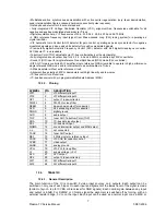
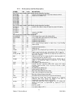
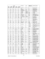
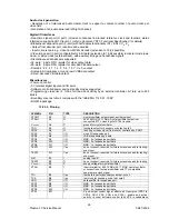
12.7.3. Pin Connections and Short Descriptions
SYMBOL PIN
TYPE
DESCRIPTION
Port 2: 8-bit programmable bidirectional port with alternative functions
P2.0/PWM 1 I/O
output for 14-bit high precision Pulse Width Modulator (PWM)
P2.1/PWM0 2 I/O
outputs for 6-bit PWMs 0 to 6
P2.2/PWM1 3 I/O
P2.3/PWM2 4 I/O
P2.4/PWM3 5 I/O
P2.5/PWM4 6 I/O
P2.6/PWM5 7 I/O
P2.7/PWM6 8 I/O
Port 3: 8-bit programmable bidirectional port with alternative functions
P3.0/ADC0
9 I/O
inputs for the software Analog-to-Digital-Converter (ADC) facility
P3.1/ADC1
10 I/O
P3.2/ADC2
11 I/O
P3.3/ADC3
12 I/O
P3.4/PWM7
30 I/O
output for 6-bit PWM7
V
SSC
13 I/O
core ground
Port 0: 8-bit programmable bidirectional port
SCL(NVRAM)
14 I
I
2
C-bus Serial Clock input to Non-Volatile RAM
SDA(NVRAM)
15 I/O
I
2
C-bus Serial Data input/output (Non-Volatile RAM)
P0.2
16 I/O
input/output for general use
P0.3
17 I/O
input/output for general use
P0.4
18 I/O
input/output for general use
P0.5
19 I/O
8 mA current sinking capability for direct drive of Light Emitting
Diodes (LEDs)
P0.6
20 I/O
P0.7
21 I/O
input/output for general use
V
SSA
22
-
analog ground
CVBS0
23 I
Composite Video Baseband Signal (CVBS) input; a positive-going
1V
CVBS1
24 I
(peak-to-peak) input is required; connected via a 100 nF capacitor
SYNC_FILTER
25 I
sync-pulse-filter input for CVBS; this pin should be connected to
V
SSA
via a 100 nF capacitor
IREF
26 I
reference current input for analog circuits; for correct operation a 24
κΩ
resistor should be connected to
V
SSA
FRAME
27 O
Frame de-interlace output synchronized with the VSYNC pulse to
produce a non-interlaced display by adjustment of the vertical
deflection circuits
TEST
28 I
not available; connect this pin to
V
SSA
COR
29 O
contrast reduction: open-drain, active LOW output which allows
selective contrast reduction of the TV picture to enhance a mixed
mode display
30 I/O
P3.4/PWM7 (described above)
V
DDA
31
-
analog supply voltage (3.3 V)
B
32 O
Blue colour information pixel rate output
G
33 O
Green colour information pixel rate output
R
34 O
Red colour information pixel rate output
VDS
35 O
video/data switch push-pull output for pixel rate fast blanking
HSYNC
36 I
horizontal sync pulse input: Schmitt triggered for a Transistor
Transistor Level (TTL) version; the polarity of this pulse is
programmable by register bit TXT1.H POLARITY
VSYNC
37 I
vertical sync pulse input; Schmitt triggered for a TTL version; the
polarity of this pulse is programmable by register bit TXT1.V
POLARITY
V
SSP
38 -
periphery ground
V
DDC
39 -
core supply voltage (+3.3 V)
Содержание 17MB11
Страница 1: ...50 PLASMA TV 17MB11 SERVICE MANUAL...
Страница 50: ...47 Plasma TV Service Manual 25 08 2005 15 CIRCUIT DIAGRAMS...
Страница 51: ...48 Plasma TV Service Manual 25 08 2005...
Страница 52: ...49 Plasma TV Service Manual 25 08 2005...
Страница 53: ...50 Plasma TV Service Manual 25 08 2005...
Страница 54: ...51 Plasma TV Service Manual 25 08 2005...
Страница 55: ...52 Plasma TV Service Manual 25 08 2005...
Страница 56: ...53 Plasma TV Service Manual 25 08 2005...
Страница 57: ...54 Plasma TV Service Manual 25 08 2005...
Страница 58: ...55 Plasma TV Service Manual 25 08 2005...
Страница 59: ...56 Plasma TV Service Manual 25 08 2005...