


14
Plasma TV Service Manual
05/01/2006
12.11. TLC7733
12.11.1. Description
The TLC77xx family of micropower supply voltage supervisors are designed for reset control, primarily
in microcomputer and microprocessor systems.
During power-on, RESET is asserted when V
DD
reaches 1 V. After minimum V
DD
(.
2 V) is established,
the circuit monitors SENSE voltage and keeps the reset outputs active as long as SENSE voltage
(V
I(SENSE)
)
remains below the threshold voltage. An internal timer delays return of the output to the inactive state to
ensure proper system reset. The delay time, t
d
, is determined by an external capacitor:
t
d
= 2.1 x 10
4
x C
T
where
C
T
is in farads
t
d
is in seconds
The TLC77xx has a fixed SENSE threshold voltage set by an internal voltage divider. When SENSE
voltage drops below the threshold voltage, the outputs become active and stay in that state until
SENSE voltage returns above threshold voltage and the delay time, t
d
, has expired.
In addition to the power-on-reset and undervoltage-supervisor function, the TLC77xx adds power-down
control support for static RAM. When CONTROL is tied to GND, RESET will act as active high. The
voltage monitor contains additional logic intended for control of static memories with battery backup
during power failure. By driving the chip select (CS) of the memory circuit with the RESET output of the
TLC77xx and with the CONTROL driven by the memory bank select signal (CSH1) of the
microprocessor (see Figure 10), the memory circuit is automatically disabled during a power loss. (In
this application the TLC77xx power has to be supplied by the battery.)
The TLC77xxQ is characterized for operation over a temperature range of –4
0°
C to 125
°
C, and the
TLC77xxI is characterized for operation over a temperature range of –40
°
C to 85
°
C.
12.12. 74LVC257A
12.12.1. Features
Wide supply voltage range of 1.2 to 3.6 V
In accordance with JEDEC standard no. 8-1A
CMOS lower power consumption
Direct interface with TTL levels
Output drive capability 50 _ transmission lines at 85°C
5 Volt tolerant inputs/outputs, for interfacing with 5 Volt logic
12.12.2. Description
The 74LVC257A is a high-performance, low-power, low-voltage, Si-gate CMOS device and superior to
most advanced CMOS compatible TTL families.
Inputs can be driven from either 3.3V or 5.0V devices. In 3-State operation, outputs can handle 5V. This
feature allows the use of these devices as translators in a mixed 3.3V/5V environment.
The 74LVC257A is a quad 2-input multiplexer with 3-state outputs, which select 4 bits of data from two
sources and are controlled by a common data select input (S). The data inputs from source 0 (1l 0 to 4l
0) are selected when input S is LOW and the data inputs from source 1 (1l 1 to 4l 1 ) are selected when
S in HIGH. Data appears at the outputs (1Y to 4Y) in true (non-inverting) form from the selected inputs.
The 74LVC257A is the logic implementation of a 4-pole, 2-position switch, where the position of the
switch is determined by the logic levels applied to S. The outputs are forced to a high impedance OFF-
state when OE is HIGH.
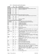
12.12.3. Pin Description
PIN NUMBER
SYMBOL
DESCRIPTION
1
S
Common data select input
2, 5, 11, 14
1
|
0
to 4
|
0
Data inputs from source 0
3, 6, 10, 13
1
|
1
to 4
|
1
Data outputs from source 1
4,7,9,12
1Y to 4Y
3-State multiplexer outputs
Содержание 17MB11
Страница 1: ...50 PLASMA TV 17MB11 SERVICE MANUAL...
Страница 50: ...47 Plasma TV Service Manual 25 08 2005 15 CIRCUIT DIAGRAMS...
Страница 51: ...48 Plasma TV Service Manual 25 08 2005...
Страница 52: ...49 Plasma TV Service Manual 25 08 2005...
Страница 53: ...50 Plasma TV Service Manual 25 08 2005...
Страница 54: ...51 Plasma TV Service Manual 25 08 2005...
Страница 55: ...52 Plasma TV Service Manual 25 08 2005...
Страница 56: ...53 Plasma TV Service Manual 25 08 2005...
Страница 57: ...54 Plasma TV Service Manual 25 08 2005...
Страница 58: ...55 Plasma TV Service Manual 25 08 2005...
Страница 59: ...56 Plasma TV Service Manual 25 08 2005...