


17
Plasma TV Service Manual
05/01/2006
• DS90C385 also available in a 64 ball, 0.8mm fine pitch ball grid array (FBGA) package
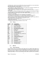
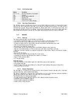
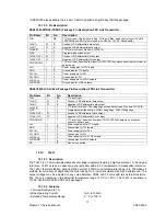
12.15.3. Pin Description
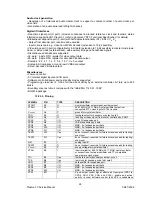
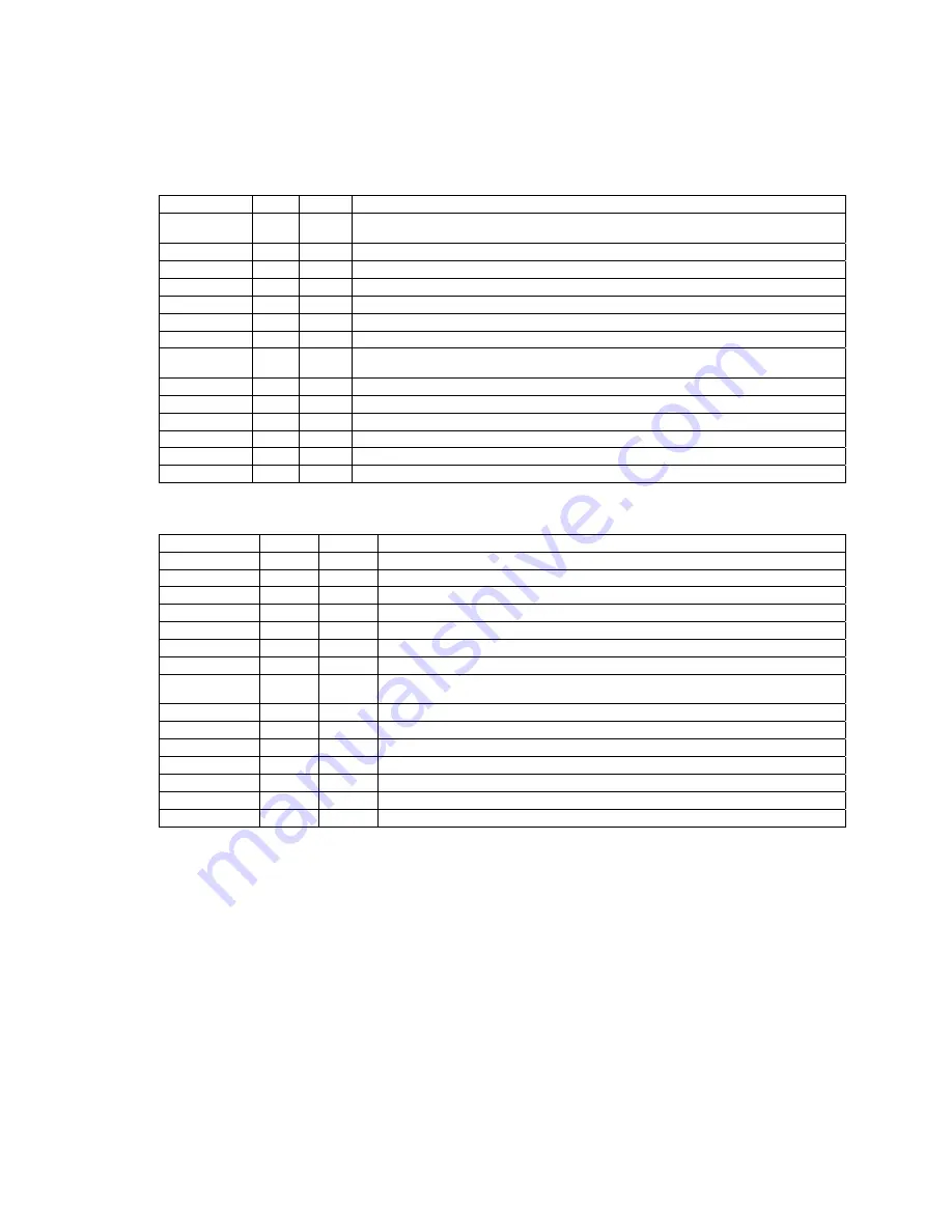
DS90C385 MTD56 (TSSOP) Package Pin Description-FPD Link Transmitter
Pin Name
I/O
No.
Description
TxIN
I 28
TTL level input. This includes: 8 Red, 8 Green, 8 Blue, and 4 control lines —FPLINE,
FPFRAME and DRDY (also referred to as HSYNC, VSYNC, Data Enable).
TxOUT+
O 4
Positive LVDS differentiaI data output.
TxOUT-
O 4
Negative LVDS differential data output.
TxCLKIN
I 1
TTL Ievel clock input. Pin name TxCLK IN.
R_FB
I 1
Programmable strobe select
TxCLK OUT+
O 1
Positive LVDS differential clock output.
TxCLK OUT-
O 1
Negative LVDS differential clock output.
PWR DOWN
I 1
TTL level input. Assertion (low input) TRI-STATES the outputs, ensuring low current at
power down.
Vcc
I 3
Power supply pins for TTL inputs.
GND
I 4
Ground pins for TTL inputs.
PLL Vcc
I 1
Power supply pin for PLL.
PLL GND
I 2
Ground pins for PLL.
LVDS Vcc
I 1
Power supply pin for LVDS outputs.
LVDS GND
I 3
Ground pins for LVDS outputs.
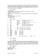
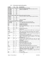
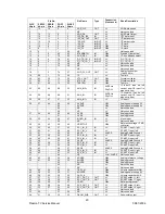
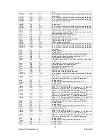
DS90C385SLC SLC64A Package Pin Description-FPD Link Transmitter
Pin Name
I/O
No.
Description
TxIN
I 28
TTL level input.
TxOUT+
O 4
Positive LVDS differentiaI data output.
TxOUT-
O 4
Negative LVDS differential data output.
TxCLKIN
I 1
TTL Ievel clock input. The rising edge acts as data strobe. Pin name TxCLK IN.
R_FB
I 1
Programmable strobe select. HIGH = rising edge, LOW = falling edge.
TxCLK OUT+
O 1
Positive LVDS differential clock output.
TxCLK OUT-
O 1
Negative LVDS differential clock output.
PWR DOWN
I 1
TTL level input. Assertion (low input) TRI-STATES the outputs, ensuring low
current at power down.
Vcc
I 3
Power supply pins for TTL inputs.
GND
I 5
Ground pins for TTL inputs.
PLL Vcc
I 1
Power supply pin for PLL.
PLL GND
I 2
Ground pins for PLL.
LVDS Vcc
I 2
Power supply pin for LVDS outputs.
LVDS GND
I 4
Ground pins for LVDS outputs.
NC
6
Pins not connected.
12.16. TL431
12.16.1. Description
The TL431 is a 3-terminal adjustable shunt voltage regulator providing a highly accurate 1 % band gap
reference. TL431 acts as an open-loop error amplifier with a 2.5V temperature compensation reference.
The TL431 thermal stability, wide operating current (150mA) and temperature range (0.to 105.makes it
suitable for all variety of application that are looking for a low cost solution with high performance. The
output voltage may be adjusted to any value between VREF and 36 volts with two external resistors.
The TL431 is operating in full industrial temperature range of 0°C to 105°C. The TL431 is available in
TO-92, SO-8, SOT-89 and SOT23-5 packages.
12.16.2. Features
• Trimmed Band gap to 1%
• Wide Operating Current
1mA to 150mA
• Extended Temperature Range
0. °C to 105.°C
Содержание 17MB11
Страница 1: ...50 PLASMA TV 17MB11 SERVICE MANUAL...
Страница 50: ...47 Plasma TV Service Manual 25 08 2005 15 CIRCUIT DIAGRAMS...
Страница 51: ...48 Plasma TV Service Manual 25 08 2005...
Страница 52: ...49 Plasma TV Service Manual 25 08 2005...
Страница 53: ...50 Plasma TV Service Manual 25 08 2005...
Страница 54: ...51 Plasma TV Service Manual 25 08 2005...
Страница 55: ...52 Plasma TV Service Manual 25 08 2005...
Страница 56: ...53 Plasma TV Service Manual 25 08 2005...
Страница 57: ...54 Plasma TV Service Manual 25 08 2005...
Страница 58: ...55 Plasma TV Service Manual 25 08 2005...
Страница 59: ...56 Plasma TV Service Manual 25 08 2005...