


23
Alignment
Receiver Alignment
RX IF Coils Alignment
r
Connect the RF Signal Generator to ANT jack, and connect
the DC voltmeter to
TP1005
on the MAIN Unit.
r
Select the “
RX IF
” channel (10.15000 MHz, CW).
r
Inject a signal from the RF Signal Generator to 10.15100
MHz, then adjust the RF Signal Generator output level so
that the DC voltmeter reading is approximately 3 V.
r
Adjust
T1008
,
T1009
,
T1010
,
T1011
,
T1012
,
T1015
,
T1016
, and
T1017
in succession several times for minimum
indication on the DC Voltmeter.
RX Gain Alignment
r
Connect the RF Signal Generator to ANT jack, and connect
the DC voltmeter to
TP1005
on the MAIN Unit.
r
Select the “
RX IF
” channel (10.15000 MHz, CW), and recall
the [
RX GAIN
] parameter on the computer.
r
Inject a signal from the RF Signal Generator to 10.15100
MHz, then adjust the RF Signal Generator output level for 6
dBµ.
r
Press the [
F10
] key to activate the
SPOT-ADJ
mode, then
press the [
S
HIFT
] + [
p
]/[
q
] keys so that the difference of the
DC Voltmeter reading is 0.1 V ±0.05 V when the RF Signal
Generator on and off.
r
Press the [
F2
] key to save the alignment value to the trans-
ceiver.
Noise Blanker Alignment
r
Connect the RF Signal Generator to ANT jack, and connect
the DC voltmeter to
TP1004
on the MAIN Unit.
r
Select the “
RX IF
” channel (10.15000 MHz, CW).
r
Inject a signal from the RF Signal Generator to 10.15100
MHz, then adjust the RF Signal Generator output level so
that the DC voltmeter reading is approximately 3 V.
r
Adjust
T1013
and
T1014
for minimum indication on the
DC Voltmeter.
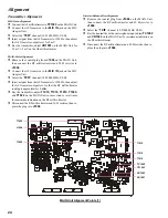
MAIN Unit Alignment Points [1]
T1017
T1016
T1015
T1012
TP1004
T1004
T1013
TP1005
T1008
T1011
T1010
T1009
Содержание VX-1210
Страница 16: ...16 Note ...
Страница 17: ...17 Block Diagram ...
Страница 18: ...18 Interconnection Diagram ...
Страница 28: ...28 Alignment Note ...
Страница 29: ...MAIN Unit 29 Circuit Diagram ...
Страница 30: ...30 MAIN Unit Note ...
Страница 44: ...44 Main Unit Note ...
Страница 45: ...CNTL Unit 45 Circuit Diagram ...
Страница 46: ...46 CNTL Unit Note ...
Страница 48: ...48 Side B 2SC2812 L6 Q2027 TC4S66F C9 Q2052 1SS319 A4 D2012 2 4 1 3 5 b a D c e d f g h CNTL Unit Parts Layout ...
Страница 56: ...56 CNTL Unit Note ...
Страница 57: ...57 PA Unit Circuit Diagram ...
Страница 58: ...58 PA Unit Note ...
Страница 60: ...60 Side B FMC5A C5 Q3001 3003 3005 MC2848 A6 D3003 3504 PA Unit Parts Layout 2 3 1 4 5 6 b a d c e f g h ...
Страница 65: ...65 Display Unit Circuit Diagram ...
Страница 70: ...70 Note ...
Страница 71: ...71 Tuner Unit ATU 1210 Option Circuit Diagram ...