

SARA-G450 - System integration manual
UBX-18046432 - R08
System description
Page 9 of 143
C1-Public
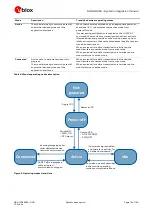
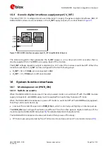
1.3
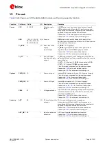
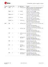
Pin-out
lists the pin-out of the SARA-G450 modules, with pins grouped by function.
Function
Pin Name Pin No
I/O Description
Remarks
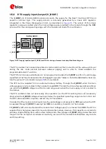
Power
VCC
51, 52, 53
I
Module supply
input
All VCC pins must be connected to external supply.
VCC supply circuit affects the RF performance and
compliance of the device integrating the module with
applicable required certification schemes.
See section
for description and requirements.
See section
for external circuit design-in.
GND
1, 3, 5, 14, 20, 22,
30, 32, 43, 50, 54,
55, 57-61, 63-96
N/A Ground
GND pins are internally connected to each other.
External ground connection affects the RF and thermal
performance of the device.
V_BCKP
2
I/O Real Time Clock
supply
input/output
V_BCKP = 3.1 V (typical).
V_BCKP is generated by internal low power linear
regulator when a valid VCC supply is present.
See section
for functional description.
See section
for external circuit design-in.
V_INT
4
O
Generic Digital
Interfaces supply
output
V_INT supply output, rail of the Digital I/O Interfaces,
generated by internal linear regulator when the module
is switched on.
V_INT = 1.8 V (typical), if VSEL is connected to GND.
V_INT = 3 V (typical), if VSEL is unconnected.
Test-Point recommended for diagnostic purpose.
See section
for functional description.
See section
for external circuit design-in.
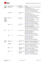
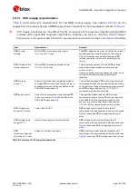
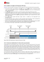
System
PWR_ON 15
I
Power-on input
Internal 28 k
active pull-up to 2.5 V internal supply.
Test-Point recommended for diagnostic purpose.
See section
for functional description.
See section
for external circuit design-in.
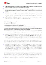
PWR_OFF 18
I
Power-off input
Internally connected to 1.5 V internal supply.
Test-Point recommended for diagnostic purpose.
See sections
for functional description.
See section
for external circuit design-in.
VSEL
21
I
Voltage selection
Input to select the operating voltage of the digital I/O
interfaces of the module (the UART interfaces, I2C
interface and GPIO pins).
See section
for functional description.
See section
for external circuit design-in.
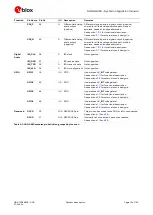
Antenna
ANT
56
I/O RF input/output for
antenna
50
nominal characteristic impedance.
Antenna circuit affects the RF performance and
compliance of the device integrating the module with
applicable required certification schemes.
See section
for description and requirements.
See section
for external circuit design-in.
ANT_DET 62
I
Input for antenna
detection
ADC input for antenna detection function.
See section
for functional description.
See section
for external circuit design-in.