SARA-G450 - System integration manual
UBX-18046432 - R08
Design-in
Page 58 of 143
C1-Public
Keep in mind that the use of rechargeable batteries requires the implementation of a suitable charger
circuit which is not included in SARA-G450 modules. The charger circuit must be designed to prevent
over-voltage on VCC pins of the module, and it should be selected according to the application
requirements: a DC-DC switching charger is the typical choice when the charging source has an high
nominal voltage (e.g. ~12 V), whereas a linear charger is the typical choice when the charging source
has a relatively low nominal voltage (~5 V). If both a permanent primary supply / charging source
(e.g. ~12 V) and a rechargeable back-up battery (e.g. 3.7 V Li-Pol) are available at the same time in the
application as possible supply source, then an appropriate charger / regulator with integrated power
path management function can be selected to supply the module while simultaneously and
independently charging the battery. See sections
for specific
design-in.
The use of a primary (not rechargeable) battery is in general uncommon, but appropriate parts can be
selected given that the most cells available are seldom capable of delivering the burst peak current
for a GSM transmission due to high internal resistance. See sections
for specific design-in.
The usage of more than one DC supply at the same time should be carefully evaluated: depending on
the supply source characteristics, different DC supply systems can result in being mutually exclusive.
The usage of a regulator or a battery not able to support the highest peak of VCC current consumption
specified in the SARA-G450 data sheet
is generally not recommended. However, if the selected
regulator or battery is not able to support the highest peak current of the module, it must be able to
support at least the highest averaged current consumption value specified in the SARA-G450 data
sheet
. The additional energy required by the module during a 2G Tx slot can be provided by an
appropriate bypass tank capacitor or supercapacitor with very large capacitance and very low ESR
placed close to the module VCC pins. Depending on the actual capability of the selected regulator or
battery, the required capacitance can be considerably larger than 1 mF and the required ESR can be
in the range of a few tens of m
. Carefully evaluate the implementation of this solution since aging
and temperature conditions significantly affect the actual capacitor characteristics.
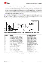
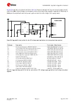
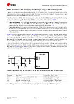
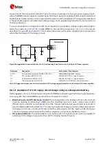
The following sections highlight some design aspects for each of the supplies listed above providing
application circuit design-in compliant with the module VCC requirements summarized in
2.2.1.2
Guidelines for VCC supply circuit design using a switching regulator
The use of a switching regulator is suggested when the difference from the available supply rail to the
VCC value is high: switching regulators provide good efficiency transforming a 12 V or greater voltage
supply to the typical 3.8 V value of the VCC supply.
The characteristics of the switching regulator connected to VCC pins should meet the following
prerequisites to comply with the module VCC requirements summarized in
Power capability: the switching regulator with its output circuit must be capable of providing a
voltage value to the VCC pins within the specified operating range and must be capable of
delivering the specified maximum peak / pulse current with 1/8 duty cycle to the VCC pins (see
SARA-G450 data sheet
Low output ripple: the switching regulator together with its output circuit must be capable of
providing a clean (low noise) VCC voltage profile.

