

SARA-G450 - System integration manual
UBX-18046432 - R08
Design-in
Page 71 of 143
C1-Public
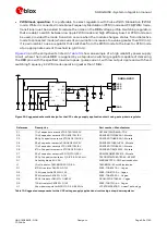
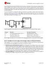
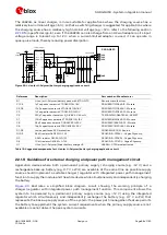
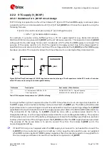
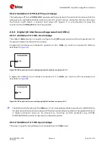
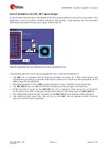
Combining a SARA-G450 cellular module with a u-blox GNSS positioning receiver, the positioning
receiver VCC supply is controlled by the cellular module by means of the “GNSS supply enable”
function provided by the set GPIO (GPIO2 as default) of the cellular module. In this case the V_BCKP
supplu output of the cellular module can be connected to the V_BCKP supply input pin of the GNSS
receiver to provide the supply for the positioning real time clock and backup RAM when the VCC
supply of the cellular module is within its operating range and the VCC supply of the GNSS receiver is
disabled. This enables the u-blox GNSS receiver to recover from a power breakdown with either a hot
start or a warm start (depending on the duration of the positioning VCC outage) and to maintain the
configuration settings saved in the backup RAM. See section
for more details regarding the
application circuit with a u-blox GNSS receiver.
☞
The internal regulator for V_BCKP is optimized for low leakage current and very light loads. Do not
apply loads which might exceed the limit for maximum available current from V_BCKP supply, as
this can cause malfunctions in the module. SARA-G450 data sheet
electrical characteristics.
V_BCKP supply output pin provides internal short circuit protection to limit start-up current and
protect the device in short circuit situations. No additional external short circuit protection is required.
☞
The ESD sensitivity rating of the V_BCKP supply pin is 1 kV (HBM as per JESD22-A114). A higher
protection level can be required if the line is externally accessible on the application PCB, e.g. if an
accessible back-up battery connector is directly connected to V_BCKP pin, and it can be achieved
by mounting an ESD protection (e.g. EPCOS CA05P4S14THSG) close to the accessible point.
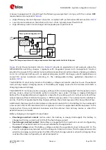
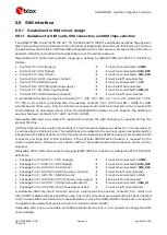
2.2.2.2
Guidelines for V_BCKP layout design
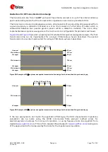
RTC supply (V_BCKP) requires careful layout: avoid injecting noise on this voltage domain as it may
affect the stability of the 32 kHz oscillator.
2.2.3
Interface supply (V_INT)
2.2.3.1
Guidelines for V_INT circuit design
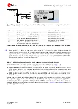
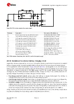
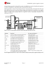
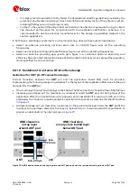
The V_INT digital interfaces 1.8 V / 3 V supply output can be mainly used to:
Indicate when the module is switched on (see sections
and
for more details)
Pull-up SIM detection signal (see section
Supply voltage translators to connect digital interfaces of the module to another voltage domain
device (see section
Pull-up DDC (I2C) interface signals (see section
Supply a 1.8 V u-blox 6 or subsequent GNSS receiver (see section
☞
Do not apply loads that might exceed the limit for maximum available current from V_INT supply,
as this can cause malfunctions in internal circuitry supplies to the same domain. SARA-G450 data
sheet
describes the detailed electrical characteristics.
☞
V_INT can only be used as an output; do not connect any external regulator on V_INT.
V_INT supply output pin provides internal short circuit protection to limit start-up current and protect
the device in short circuit situations. No additional external short circuit protection is required.
☞
ESD sensitivity rating of the V_INT supply pin is 1 kV (HBM according to JESD22-A114). A higher
protection level could be required if the line is externally accessible on the application PCB. A higher
protection level can be achieved by mounting an ESD protection (e.g. EPCOS CA05P4S14THSG
varistor array) close to accessible points.


