SARA-G3 series - System Integration Manual
UBX-13000995 - R06
Objective Specification
Design-in
Page 123 of 218
Limit capacitance and series resistance on each SIM signal (
SIM_CLK
,
SIM_IO
,
SIM_RST
) to match
the requirements for the SIM interface (27.7 ns is the maximum allowed rise time on the
SIM_CLK
line, 1.0 µs is the maximum allowed rise time on the
SIM_IO
and
SIM_RST
lines)
SARA-G3 series
41
VSIM
39
SIM _IO
38
SIM _CLK
40
SIM _RST
4
V_INT
42
SIM _DET
SIM CARD
HOLDER
C
5
C
6
C
7
C
1
C
2
C
3
SIM Card
Bottom View
(contacts side)
C1
VPP (C6)
VCC (C1)
IO (C7)
CLK (C3)
RST (C2)
GND (C5)
C2
C3
C5
J1
C4
D1 D2 D3 D4
C
8
C
4
TP
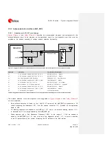
Figure 43: Application circuit for the connection to a single removable SIM card, with SIM detection not implemented
Reference
Description
Part Number - Manufacturer
C1, C2, C3, C4
47 pF Capacitor Ceramic C0G 0402 5% 50 V
GRM1555C1H470JA01 - Murata
C5
100 nF Capacitor Ceramic X7R 0402 10% 16 V GRM155R71C104KA01 - Murata
D1, D2, D3, D4
Very Low Capacitance ESD Protection
PESD0402-140 - Tyco Electronics
J1
SIM Card Holder
6 positions, without card presence switch
Various Manufacturers,
C707 10M006 136 2 - Amphenol
Table 23: Example of components for the connection to a single removable SIM card, with SIM detection not implemented
Guidelines for single SIM chip connection
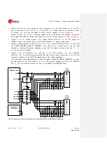
A solderable SIM chip (M2M UICC Form Factor) must be connected the SIM card interface of SARA-G3
modules as described in
, where the optional SIM detection feature is not implemented
(refer to the circuit described in
if the SIM detection feature is not required).
Follow these guidelines connecting the module to a solderable SIM chip without SIM presence detection:
Connect the UICC / SIM contacts C1 (VCC) and C6 (VPP) to the
VSIM
pin of the module
Connect the UICC / SIM contact C7 (I/O) to the
SIM_IO
pin of the module
Connect the UICC / SIM contact C3 (CLK) to the
SIM_CLK
pin of the module
Connect the UICC / SIM contact C2 (RST) to the
SIM_RST
pin of the module
Connect the UICC / SIM contact C5 (GND) to ground
Provide a 100 nF bypass capacitor (e.g. Murata GRM155R71C104K) at the SIM supply line (
VSIM
)
close to the relevant pad of the SIM chip, to prevent digital noise
Provide a bypass capacitor of about 22 pF to 47 pF (e.g. Murata GRM1555C1H470J) on each SIM
line (
VSIM
,
SIM_CLK
,
SIM_IO
,
SIM_RST
), to prevent RF coupling especially in case the RF
antenna is placed closer than 10 - 30 cm from the SIM card holder
Limit capacitance and series resistance on each SIM signal (
SIM_CLK
,
SIM_IO
,
SIM_RST
) to match
the requirements for the SIM interface (27.7 ns is the maximum allowed rise time on the
SIM_CLK
line, 1.0 µs is the maximum allowed rise time on the
SIM_IO
and
SIM_RST
lines)


