SARA-G3 series - System Integration Manual
UBX-13000995 - R06
Objective Specification
Appendix
Page 208 of 218
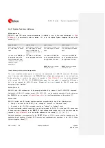
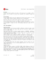
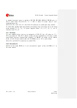
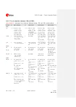
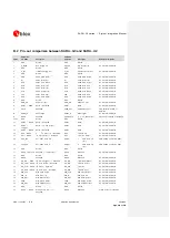
B.2
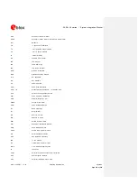
Pin-out comparison between SARA-G3 and SARA-U2
SARA-G3
SARA-U2
Pin No
Pin Name
Description
Pin Name
Description
Remarks for migration
1
GND
Ground
GND
Ground
2
V_BCKP
RTC Supply I/O
V_BCKP
RTC Supply I/O
No functional difference
3
GND
Ground
GND
Ground
4
V_INT
Interfaces Supply Out
V_INT
Interfaces Supply Out
No functional difference
5
GND
Ground
GND
Ground
6
DSR
UART DSR Output
DSR
UART DSR Output
No functional difference
7
RI
UART RI Output
RI
UART RI Output
No functional difference
8
DCD
UART DCD Output
DCD
UART DCD Output
No functional difference
9
DTR
UART DTR Input
DTR
UART DTR Input
No functional difference
10
RTS
UART RTS Input
RTS
UART RTS Input
No functional difference
11
CTS
UART CTS Output
CTS
UART CTS Output
No functional difference
12
TXD
UART Data Input
TXD
UART Data Input
No functional difference
13
RXD
UART Data Output
RXD
UART Data Output
No functional difference
14
GND
Ground
GND
Ground
15
PWR_ON
Power-on Input
PWR_ON
Power-on Input
No functional difference
16
GPIO1 / RSVD
GPIO / Reserved
GPIO1
GPIO
No functional difference
17
RSVD
Reserved
VUSB_DET
USB Detect Input
USB detection instead of
Reserved
18
RESET_N
Reset signal
RESET_N
Reset signal
No functional difference
19
RSVD
Reserved
CODEC_CLK
13 or 26 MHz Output
Clock output instead of Reserved
20-22
GND
Ground
GND
Ground
23
GPIO2 / RSVD
GPIO / Reserved
GPIO2
GPIO
No functional difference
24
GPIO3 /
32K_OUT
GPIO / 32 kHz Output
GPIO3
GPIO
No functional difference
25
GPIO4 / RSVD
GPIO / Reserved
GPIO4
GPIO
No functional difference
26
SDA / RSVD
6
I
2
C Data I/O / Reserved
SDA
I
2
C Data I/O
No functional difference
27
SCL / RSVD
I
2
C Clock Output / Reserved
SCL
I
2
C Clock Output
No functional difference
28
RXD_AUX
Aux UART Data Out
USB_D-
7
USB Data I/O
(D-)
USB instead of Auxiliary UART
29
TXD_AUX
Aux UART Data In
USB_D+
8
USB Data I/O
(D+)
USB instead of Auxiliary UART
30
GND
Ground
GND
Ground
31
RSVD / EXT32K Reserved / 32 kHz Input
RSVD
Reserved
No functional difference
32
GND
Ground
GND
Ground
33
RSVD
Reserved
RSVD
Reserved
No functional difference
34
I2S_WA / RSVD I
2
S Word Alignment / Reserved
I2S_WA
I
2
S Word Alignment
No functional difference
35
I2S_TXD / RSVD I
2
S Data Output / Reserved
I2S_TXD
I
2
S Data Output
No functional difference
36
I2S_CLK / RSVD I
2
S Clock / Reserved
I2S_CLK
I
2
S Clock
No functional difference
37
I2S_RXD / RSVD I
2
S Data Input / Reserved
I2S_RXD
I
2
S Data Input
No functional difference
38
SIM_CLK
SIM Clock Output
SIM_CLK
SIM Clock Output
No functional difference
39
SIM_IO
SIM Data I/O
SIM_IO
SIM Data I/O
No functional difference
40
SIM_RST
SIM Reset Output
SIM_RST
SIM Reset Output
No functional difference
41
VSIM
SIM Supply Output
VSIM
SIM Supply Output
No functional difference
42
SIM_DET
SIM Detection Input
SIM_DET
SIM Detection Input
No functional difference
43
GND
Ground
GND
Ground
44
SPK_P / RSVD Analog Audio Out (+) /
Reserved
RSVD
Reserved
Analog audio not supported

