background image

www.ti.com

Software Control

2.2.4.3

Clock Output Controls

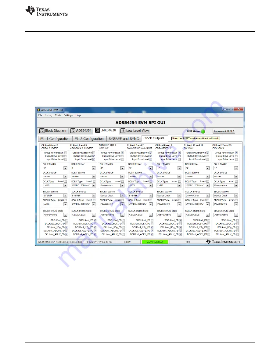
Clicking

Clock Outputs

opens the LMK04828 Clock Outputs tab, shown in

Figure 7

This tab is organized

into 7 sections representing the 7 pairs of DCLK/SYSREF that the LMK04828 can generate. For each of
the 7 pairs of DCLK/SYSREF, there are a number of controls that apply to both outputs, such as the
option to power down the pair of signals completely, if not needed. For both DCLK and SYSREF, there is
an option to select what type of output driver is to be used, such as LVDS or LVPECL. There are controls
to enable things like delay or inversion. For the DCLK, there is a control to select a divider ration to divide
the PLL2 VCO clock down to the desired output frequency. For example, if the ADS54J54 EVM is to be
operated at 500 Msps, then the configuration file supplied with the GUI will select the 3.0-GHz VCO and
select a divider ratio of 6 to generate a 500-MHz DCLK. If the TSW14J56 capture card is used, the
TSW14J56 needs to see a DCLK reference that is one-twentieth the line rate of the serial data stream so
the divider ratio chosen is 12 to generate a 250-MHz DCLK to the FMC connector. These two divider
ratios can be seen in

Figure 7

.

Figure 7. LMK04828 Clock Outputs Tab

11

SLAU616A – January 2015 – Revised January 2016

ADS54J54 Evaluation Module

Submit Documentation Feedback

Copyright © 2015–2016, Texas Instruments Incorporated

Содержание ADS54J54EVM

Страница 1: ...ter Pro GUI software The EVM schematics BOMs and layout files are found in the design package under the ADS54J54EVM tool folder on www ti com Contents 1 Introduction 2 1 1 Overview 2 1 2 Block Diagram...

Страница 2: ...sample clock for the mating FPGA capture board for a complete JESD204B subclass 1 clocking solution The ADS54J54 and LMK04828 are controlled through an easy to use software GUI enabling quick configu...

Страница 3: ...r ADS54J54 J26 TRIG_OUT Trigger output buffered version of ADS58J89 burst mode trigger normally connected to trigger input of TSW14J56 capture card Normally not used for ADS54J54 J7 LMK CLKIN1_P CLKIN...

Страница 4: ...e drivers follow the prompts on the screen to do so Do not let Windows XP search Microsoft Update for the drivers but do let Windows XP install the drivers automatically Windows 7 After installing the...

Страница 5: ...DI button will attempt to reestablish the USB link between the PC and the EVM For the GUI to operate correctly it is important that the ADS54J54 and LMK04828 each be reset by clicking on the respectiv...

Страница 6: ...B or channels C and D respectively CLK SEL AB and CD Selects the clock input for channels A and B or for channels C and D respectively CLK Phase SEL AB and CD Selects the phase relationship of the clo...

Страница 7: ...channels C and D Test Pattern Selects the specific test pattern to be output when test pattern is selected PRBS Select Selects the length of the PRBS test pattern PRBS Enable Selects the PRBS test pat...

Страница 8: ...DS54J54 is a four channel device then M is assumed to be 4 The parameter L refers to the number of lanes used The ADS54J54 may use one lane per channel when in 2x decimation mode to output 250 Msps or...

Страница 9: ...rnal reference frequency from PLL1 and from this VCO the output clocks are generated Figure 5 LMK04828 PLL1 Configuration Tab 2 2 4 1 PLL1 Configuration Much of this panel is organized in block diagra...

Страница 10: ...airs is connected to the FMC connector to source DCLK SYSREF to the FPGA on the TSW14J56 capture card Another DCLK SYSREF pair is used to clock the ADS54J54 The other 5 pairs of clocks are normally po...

Страница 11: ...rsion For the DCLK there is a control to select a divider ration to divide the PLL2 VCO clock down to the desired output frequency For example if the ADS54J54 EVM is to be operated at 500 Msps then th...

Страница 12: ...REF rate to the Local MultiFrame Clock period or LMFC period For the default configuration of the ADS54J54 EVM as configured by the ADS54J54_500M_LMF881 config file the device is set up for 2 lanes pe...

Страница 13: ...bit 4 of address 0x00 is the bit to choose between 3 wire SPI or 4 wire SPI for the LMK04828 To set a bit to a 1 check the box for that bit in the W column then click Write Register The GUI will writ...

Страница 14: ...gnal source The clock source is from the LMK04828 but the board provides an option to use an external clock source such as a HP8644B for the ADC sample clock Note that a narrow bandpass filter is reco...

Страница 15: ...h SW6 to the ON position 3 Insert a USB cable into the USB port on the TSW14J56 Connect the other end to the PC 3 3 2 ADS54J54EVM 1 Connect a bench 5 V power supply or equivalent to the connector J13...

Страница 16: ...PLL s of the LMK04828 should now be locked This is indicated on the ADS54J54 circuit board by the illuminated LED s D4 PLL2 LOCKED and D1 labeled LMK LOCKED 7 The TSW14J56 capture card should now be r...

Страница 17: ...e coherent then select Auto Calculation of Coherent Frequencies 6 If a windowing function is desired then Blackman should be selected above the plot window If the clocks are synchronized with an exter...

Страница 18: ...ing the warranty period to the address designated by TI and that are determined by TI not to conform to such warranty If TI elects to repair or replace such EVM TI shall have a reasonable time to repa...

Страница 19: ...transmitter has been approved by Industry Canada to operate with the antenna types listed in the user guide with the maximum permissible gain and required antenna impedance for each antenna type indic...

Страница 20: ...ified allowable ranges some circuit components may have elevated case temperatures These components include but are not limited to linear regulators switching transistors pass transistors current sens...

Страница 21: ...REMOVAL OR REINSTALLATION ANCILLARY COSTS TO THE PROCUREMENT OF SUBSTITUTE GOODS OR SERVICES RETESTING OUTSIDE COMPUTER TIME LABOR COSTS LOSS OF GOODWILL LOSS OF PROFITS LOSS OF SAVINGS LOSS OF USE L...

Страница 22: ...sponsible for compliance with all legal regulatory and safety related requirements concerning its products and any use of TI components in its applications notwithstanding any applications related inf...

Отзывы: