


TAMC900 User Manual Issue 2.0.1
Page 14 of 71
4 Functional Procedures
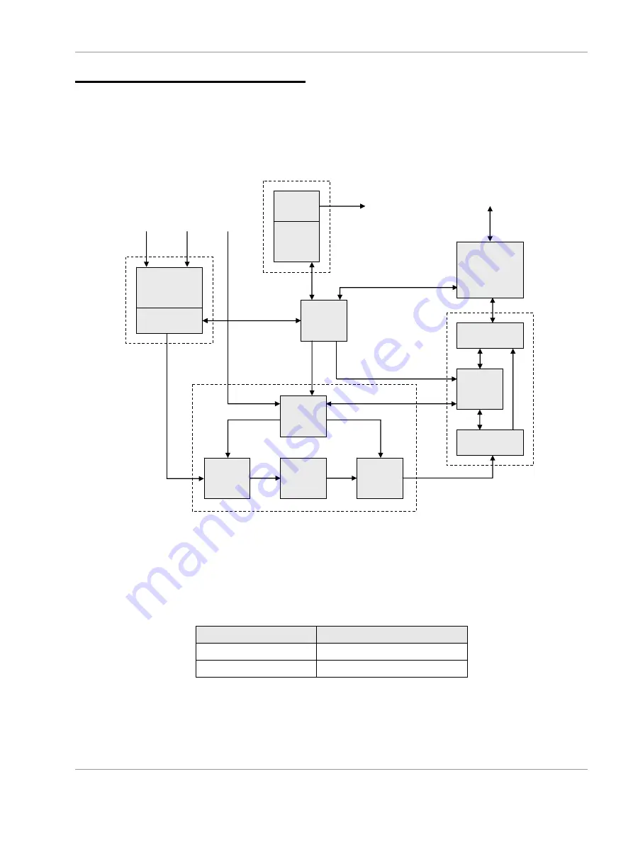
The following diagram illustrates the structure of the ADC data acquisition system implemented on the
TAMC900. The structure is abstract in order to show the different functional units and the data flow. All
physical connections are termed in a bold style. The remaining ones are internal connections.
The functional units are described in the subsequent chapters.
Data
Steering
ADC
Synchronisation
FIFO
Sign Extension
QDR-II
Memory
Data
Steering
Operation
Modes
Registers
Channel FIFO
DMA Engine (x8)
Tracking Buffer (x2)
Channel Logic (x2)
DCMs
AMC PCI Express
Connection
ADC
Inputs
Control
Logic
Clock
Distribution
Sample Rate Logic
Trigger
Inputs
Sampling
Clocks
DMA
Logic
PCI Express
Endpoint
Transmit Buffer
Figure 4-1: TAMC900 FPGA System Structure
The physical clocking structure of the TAMC900 results in two different (ADC) channel groups. The module
contains eight separate 14 bit ADC channels that are structured in the way: two times four. The ADC-to-
channel group assignment is shown in the subsequent table.
Channel Group
Corresponding ADC(s)
0 0-3
1 4-7
Table 4-1: ADC Channel Group Assignment
Each group has restrictions concerning a common sampling clock and a common trigger configuration.