31
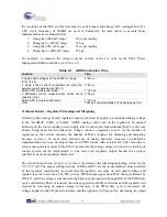
the resolution of the ADC and the time taken to switch inputs and change ADC configuration. At a
CPU clock frequency of 24MHz (as used in Example2), the time taken to execute those
fundamental tasks is outlined below:
1.
Using the ±2048 mV range:
65
μ
s per reading
2.
Changing to ±256mV range:
320
μ
s
3.
Using the ±256 mV range:
83
μ
s per reading
4.
Changing to ±2048 mV range: 320
μ
s
For example, to measure the voltage and the current of the 4+1 rails on the PSoC Power
Management EBK would take: (see
Table 4-1
)
Table 4-1 ADC Conversion Time
Function
Time
5 single ended voltages on the ±2048 mV range
(VIN, V1-V4)
5* 65
μ
s
2 single ended current measurements using the
external current sense amps (IIN, I1)
2* 65
μ
s
Switch ADC to differential mode
1* 320
μ
s
3 differential current measurements across shunt
resistors (I2-I4)
3* 83
μ
s
Switch ADC to single ended mode
1* 320
μ
s
Total 1344
μ
s or approximately 270
μ
s average per rail
Technical Details – Regulator Trimming and Margining
Trimming (fine tuning) of each regulator output is achieved by applying a controlled analog voltage
to the “feedback” (VFB) or “adjust” (VADJ) analog control pin on the regulators. To support
trimming on the four secondary power supply rails would require four additional DACs to the ones
already being used for the under/over voltage window comparator circuit. As the number of
regulators in the systems expands, the number of DACs required for trimming and margining
becomes excessive. To make more efficient use of analog hardware resources, an alternative
implementation has been developed based on PWM blocks with external RC filter networks to
achieve the equivalent result. Since PSoC can measure the analog voltage of each rail, a closed loop
control system can be implemented to fine tune each regulator output beyond the accuracy
specifications of the regulators themselves.
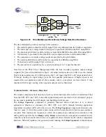
The circuit shown below (
Figure 4-24
) shows the detail of the trimming/margining circuit for the
V3=2.5 V rail. The output scaling network of R46 and R51 are the recommended values provided
by the regulator manufacturer to ensure that the regulator can sense its own output voltage and
regulate it as the load varies. The TR3 pin is a PWM output signal from PSoC that gets filtered by
R54/C15 and that voltage is summed into the FB pin of the regulator through R50. If the PWM duty
cycle controlled by PSoC is reduced, the voltage applied to the FB will reduce and the regulator will
respond by increasing its output voltage. Conversely, if the PWM duty cycle is increased, the
voltage applied to the FB pin will increase and the regulator will respond by decreasing its output
Содержание CY8CKIT-035
Страница 1: ......
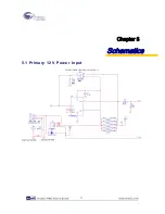
Страница 38: ...Chapter 5 Schematics 5 1 Primary 12V Power Input 37 ...
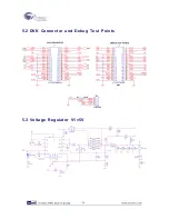
Страница 39: ...5 2 DVK Connector and Debug Test Points 5 3 Voltage Regulator V1 5V 38 ...
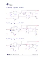
Страница 40: ...5 4 Voltage Regulator V2 3 3V 5 5 Voltage Regulator V3 2 5V 5 6 Voltage Regulator V4 1 8V 39 ...
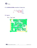
Страница 41: ...5 7 I2C SMBus PMBus Interface Connector 5 8 Layout 5 8 1 Top Layer 40 ...
Страница 42: ...5 8 2 Ground Layer 5 8 3 Power Layer 41 ...
Страница 43: ...5 8 4 Bottom Layer 42 ...
Страница 44: ...5 8 5 Top Silkscreen 43 ...

