12
3.2
PME EBK Headers and Jumpers
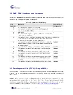
A number of headers and jumpers are provided on the PME EBK. The following table outlines the
function of each item and the default configuration.
Table 3-2 PME Jumper Settings
PCB
Designator
Description
Factory Default
Configuration
J1
2×20 pin header for connecting to PSoC DVK
-
J2
5-pin header for connecting an external host or management
processor via I2C/SMBus/PMBus
-
J3 Power
Jack
-
J4
2×20 pin header that replicates signals on J1 for easy connection to a
logic analyzer or oscilloscope
-
J5
3-pin header for primary input power source selection. Place jumper in
1-2 position to source power from the DC power jack J3. Place in 2-3
position to source power from the PSoC platform DVK
2-3 position
J6
2-pin header for connecting all loads on V1=5V rail (this includes the
fixed and adjustable loads on V1 as well as the load presented by the
V2, V3 and V4 rails)
Installed
J7
2-pin header for connecting the potentiometer load on V1=5V rail
Installed
J8
2-pin header for connecting both loads on V2=3.3V rail (fixed and
adjustable)
Installed
J9
2-pin header for connecting potentiometer load on V2=3.3V rail
Installed
J10
2-pin header for connecting ALL loads on V3=2.5V rail (fixed and
adjustable)
Installed
J11
2-pin header for connecting variable potentiometer on V3=2.5V rail
Installed
J12
2-pin header for connecting ALL loads on V4=1.8V rail (fixed and
adjustable)
Installed
J13
2-pin header for connecting variable potentiometer on V4=1.8V rail
Installed
3.3
Development Kit (DVK) Compatibility
This kit contains an expansion board only and requires a Cypress development kit platform in order
to use it. This kit is compatible with both the CY8CKIT-001 PSoC DVK and the CY8CKIT-030
PSoC 3 DVK.
NOTE:
Early revisions of the CY8CKIT-001 PSoC Development Kit contained an early
engineering sample release (ES2) of the PSoC 3 CY8C38xxx Device Family Processor Module
which is not compatible with the example projects that accompany this kit. If you have an early
revision of the kit you can upgrade free of charge at
www.cypress.com/go/psoc3kitupgrade
.
Содержание CY8CKIT-035
Страница 1: ......
Страница 38: ...Chapter 5 Schematics 5 1 Primary 12V Power Input 37 ...
Страница 39: ...5 2 DVK Connector and Debug Test Points 5 3 Voltage Regulator V1 5V 38 ...
Страница 40: ...5 4 Voltage Regulator V2 3 3V 5 5 Voltage Regulator V3 2 5V 5 6 Voltage Regulator V4 1 8V 39 ...
Страница 41: ...5 7 I2C SMBus PMBus Interface Connector 5 8 Layout 5 8 1 Top Layer 40 ...
Страница 42: ...5 8 2 Ground Layer 5 8 3 Power Layer 41 ...
Страница 43: ...5 8 4 Bottom Layer 42 ...
Страница 44: ...5 8 5 Top Silkscreen 43 ...


