5
( )
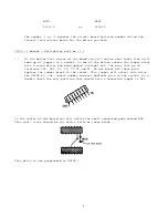
On the other drive bend straight the pins going to DS1 and DS3 - all others
should be left as they are to complete the jumpering of DS2, T1, T2, T3, T4
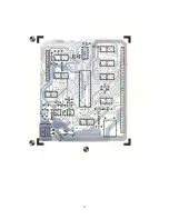
and T5. Re-install the jumper block. In the center of the board you will
notice two small connected pads marked MUX. This small trace should be cut
with a knife or razor blade.
This drive is now programmed as DRIVE #1.
( )
Go on to the final assembly instructions.
25060 -2 boards ( Both drives must be -2 )
( )
At the bottom left corner of the board you will notice what looks like an IC
made up of jumpers in a socket. On cane of the drives remove the jumper block
with a screwdriver and bend upward (straight ) the pins that go to terminals
DS2, DS3, and MX. not break these pins off. Re-install the jumper block into
the socket. As a double check the jumper block should have pins inserted only
in terminals DS1, HS and the unlabeled pin. There should be nothing plugged
into the HM position.
Directly above this jumper block you will notice what appears to be a 14 pin
IC in a socket. This is not an IC but is an array of pull-up resistors.
Carefully remove this array from its socket using a small screwdriver. This
array should not be reinstalled. This drive is now programmed as DRIVE 0.
( )
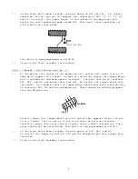
On the other drive bend straight the pins going to DS1, DS3, and MX.
Re-install the jumper so that HS, DS2 and the unlabeled pin have jumper pins
installed.
( )
Go on to the final assembly instructions.


