47
NW-A1000
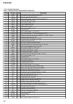
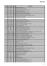
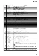
Pin No.
Pin Name
I/O
Description
52
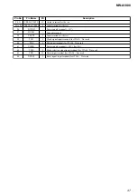
CRST1
O
External capacitor connection terminal for reset delay (for XRST1)
53
CRST2
O
External capacitor connection terminal for reset delay (for XRST2)
54
CRST3
O
External capacitor connection terminal for reset delay (for XRST3)
55
SEQSEL
I
LDO output trigger selection signal input terminal "L": VO interlock, "H": XRST interlock
Fixed at "L" in this set
56
SEL1
I
LDO1 and LDO3 power output control selection signal input terminal
"L": When VBUS is detected, power is output, "H": power is always output
Fixed at "H" in this set
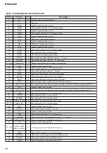
57
SEL2
I
LDO1 and LDO3 power output control selection signal input terminal
"L": according to the setting of SEL1, "H": power is output at a normal sequence
Fixed at "H" in this set
58
DCIN_MON
I
DC power input monitor input terminal
59
VBUSIN
I
VBUS power supply input terminal (+5V)
60
VBUS_LIM
I
USB current limit control signal input from the PLD "L": 100 mA, "H": 500 mA
61
VBATT
I
Battery power supply input terminal (+3.7V)
62
BATTMON
O
Battery voltage monitor output to the main system controller
63
BATTMON_CTL
I
Battery voltage monitor on/off control signal input from the PLD
"H": battery voltage monitor on
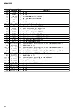
64
XDCIN_DET
O
DC power detection signal output terminal
65
XVBUS_DET
O
VBUS power detection signal output terminal
66
VBUSSUSPEND
I
Setting terminal for the USB suspend mode "H": USB suspend mode
67
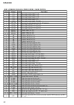
XCHG_STAT1
O
Charging flag output terminal "L" active
68
XCHG_STAT2
O
Charge completion flag output terminal "L" active
69
TS
I
Temperature sensor input terminal
70
LOGIC_H
I
Power supply input terminal (+3V) (for logic "H")
71
CS
I
Chip select signal input from the PLD "H" active
72
SCK
I
Serial data transfer clock signal input from the PLD
73
SI
I
Serial data input from the PLD
74
SO
O
Serial data output to the main system controller
75
XGND_SW
O
Ground switch terminal for the remote commander
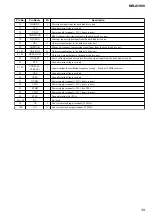
76
GPIO0
O
DC power on/off control signal output terminal "H": power on
77
GPIO1
O
Charge on/off control signal output terminal "L": charge on
78
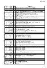
RST
O
System reset signal input from the reset switch "L": reset
For several hundreds msec. after the power supply rises, "L" is input, then it change to "H"
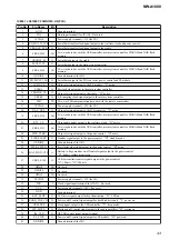
79
RMON11
I
External resistor return terminal
80
RMON12
I
External resistor return terminal
81
RMON21
I
External resistor return terminal
82
RMON22
I
External resistor return terminal
83
GATE1
O
VBUS or DC/battery power selection signal output terminal
"L": battery power, "H": VBUS or DC power
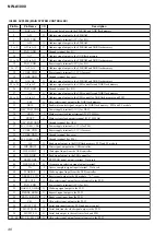
84, 85
GATE2, GATE3
O
Battery power on/off control signal output terminal "H": power on
86
CHGREG
O
Reference voltage (+2.4V) output terminal for charge circuit
87, 88
VCC
-
Power supply terminal (+3.7V)
89 to 91
GND
-
Ground terminal
92
BGGND
-
Ground terminal (for BG)
93
DISGND
-
Ground terminal (for discharge)
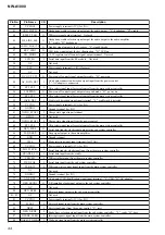
94 to 96
TEST1 to TEST3
I
Input terminal for the test mode setting
97
TEST4
O
Output terminal for the test mode setting
98 to 100
NC
-
Not used

