43
NW-A1000
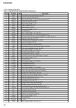
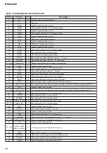
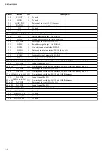
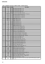
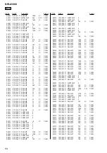
IC8001 LC4128ZC-75MN132C-U5 (PLD)
Pin No.
Pin Name
I/O
Description
1
GND
-
Ground terminal
2
TDI
I
Data input terminal (for JTAG) Not used
3
VCCIO0
-
Power supply terminal (+3V) (for I/O)
4
EX_MULTI_SCK
O
Serial data transfer clock signal output to the real time clock and power control
5
CRADLE_SCK
O
Serial data transfer clock signal output to the cradle
6
FRES_D28
I/O
Two-way data bus with the USB controller, main system controller, SD-RAM and NOR flash
memory
7
CRADLE_SI
O
Serial data output to the cradle
8
MULTI_SI
O
Serial data output to the main system controller
9
FRES_D29
I/O
Two-way data bus with the USB controller, main system controller, SD-RAM and NOR flash
memory
10
GNDIO0
-
Ground terminal (for I/O)
11
EX_MULTI_SO
O
Serial data output to the D/A converter, power control and EL module
12
LCD_XCS
O
Chip select signal output to the EL module "L" active
13
SCLK1
O
Bit clock signal output to the main system controller
14
CRADLE_CS
O
Chip select signal output to the cradle "H" active
15
LRCK1
O
L/R sampling clock signal output to the main system controller
16
TSB
I/O
Two-way TSB communication data bus with the remote commander
17
VCCIO0
-
Power supply terminal (+3V) (for I/O)
18
DAC_XCS
O
Chip select signal output to the D/A converter "L" active
19
FRES_D30
I/O
Two-way data bus with the USB controller, main system controller, SD-RAM and NOR flash
memory
20
RTC_CE
O
Chip enable signal output to the real time clock "H" active
21
FRES_D31
I/O
Two-way data bus with the USB controller, main system controller, SD-RAM and NOR flash
memory
22
PWR_STRB
O
Chip select signal output to the power control "H" active
23
PWR_SLEEP
O
Standby signal output to the power control "H": standby mode
24
GNDIO0
-
Ground terminal (for I/O)
25
PWR_FFCLR
O
Start factor clear signal output to the power control "H" active
26
BAT_MON_CTL
O
Battery voltage monitor on/off control signal output to the power control
"H": battery voltage monitor on
27
VBUS_LIM
O
USB current limit control signal output to the power control
"L": 100 mA, "H": 500 mA
28
GPIO8
I/O
Not used
29
GPIO20
O
Not used
30
GPIO9
I/O
Not used
31
VCCIO0
-
Power supply terminal (+3V) (for I/O)
32
TCK
I
Clock signal input terminal (for JTAG) Not used
33
VCC
-
Power supply terminal (+1.8V) (for core)
34
GND
-
Ground terminal
35
KEY_LED2
O
LED drive signal output for key illumination "H": LED on
36
XHDD_PWR_CTL
O
Power on/off control signal output for hard disk drive unit "L": power on
37
XUSLEEP
O
Sleep signal output to the USB controller "L": sleep mode
38
HP_MUTE
O
Muting on/off control signal output to the audio amplifier "H": muting on
39
IIS_CLR
O
IIS CLR control signal output terminal
40
EL_PWR
O
Power on/off control signal output for EL module "H": power on
41
GNDIO0
-
Ground terminal (for I/O)

