background image

SECTION  2 

DISASSEMBLY 

KVX-370 

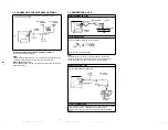
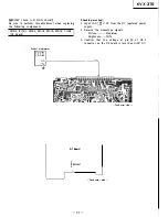
2-1.  REMOVAL  OF  REAR  LID

two  claws. 

®  Remove  the  rear  lid. 

*

Remove  it  while  holding  the
portion  of  the 

antenna

indicated  by  the  arrow  ©.

®  Set  up 

the  antenna. 

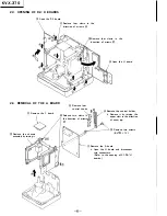
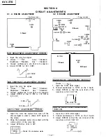
2-2.  REMOVAL  OF  J/D3/M  BOARDS

®  Remove 

®  Remove  three  screws 

(BVTP3 

10). 

@)  Remove  the  heat 

-7-

(J)  Remove  it  by  pressing  two 

claws  in  the  direction  of 

arrows @. 

@  Remove  the  D3  board. 

*

Remove  its  upper  first. 

G)  Remove  the  antenna  holder 

panel. 

by  pressing 

two  claws  in  the 

@  Remove  two  claws 

(BVTP3 

12). 

®  Remove  the  screw 

(BVTP3 

12). 

--.....__'-;--...,.J 

@  Remove  the  J  board. 

*

Remove  it  while  pulling
the  claw  side. 

@  Remove  the  M  board. 

*

Remove  it  by pressing  two 
claws  indicated  with  the 
circle  on  the  M  board  in 
the  direction  of  arrows 

©.

Содержание KV-4SV1

Страница 1: ...C DC IN 12 V jack accepts AC 42 AC power adaptor supplied for use on 120 V AC 60 Hz DCC 16AW car battery cord optional for use on 12 V battery Power consumption Dimensions Weight 1 AC 42 AC power adaptór Rated input voltage Nominal output voltage Rated output current Power consumption Cord length 15 6 W 133 x 133 x 152 mm w h d 51 4 x 5 x 6 inches incl projecting paris and controls Approx 1 3 kg 2...

Страница 2: ...GRAMS 5 1 Block Diagram 17 5 2 Circuit Boards Location 25 5 3 Printed Wiring Boards and Schematic Diagram 25 5 4 Semiconductors 61 6 EXPLODED VIEWS 1 Chassis 62 2 Picture Tube 63 7 ELECTRICAL PARTS LIST 64 WARNING AN ISOLATION TRANSFORMER SHOULD BE USED DURING ANY SERVICE TO AVOID POSSIBLE SHOCK HAZARD BECAUSE OF LIVE CHASSIS THE CHASSIS OF THIS RECEIVER IS DIRECTLY CON NECTED TO THE AC POWER LINE...

Страница 3: ...low 0 15µF To Exposed Metal Parts on Set 1 5kr Earth Ground AC voltmeter 0 75V Fig A Using an AC voltmeter to check AC leakage 3 LEAKAGE TEST The AC leakage from any exposed metal part to earth ground and from all exposed metal parts to any exposed metal part having a return to chassis must not exceed 0 5 mA 500 microampers Leakage current can be measured by any one of three methods 1 A commercial...

Страница 4: ...lease The time is displayed while the birds move across the screen for approx 10 seconds 0 AM 3 28 When the unit is turned on for the first time or after being left with the power disconnected for more that one day the time indication will show When you press the HOUR or MINUTE button once the indication changes to 12 00 AM Note on time indication 12 00 AM Midnight 12 00 PM Noon 1 3 TO WAKE UP TO ...

Страница 5: ...he CHANNEL or button 4 L 0 CHANNELD 4 Press TUN NG or button D t w I The program oi channel 42 When you press the button once the TV will search for the channels and stops ai lhe nearest channel Press lhe button repeatedly until a program of the desired channel appears on the screen 5 Sei the function selector to CHANNEL SET 1 CHANNEL SET tL 6 Press CHANNEL SET INDICATOR or To change lhe tens digi...

Страница 6: ...IN Jacks VMC 710M 720M optional VIDEO to video 1l selector output to audio output 1 1 ol L_j i ll VCR To view playback picture 1 Set the VIDEO TV selector on the rear to VIDEO I VIDEO TV 2 Set the VCR in the playback mode Notes Before connection turn off the TV and the equipment to be connected Make firm connections A loose connection may cause a distorted picture Keep the VCR away from the TV if ...

Страница 7: ... BVTP3 x 10 Remove the heat 7 J Remove it by pressing two claws in the direction of arrows Remove the D3 board Remove its upper first G Remove the antenna holder panel by pressing two claws in the Remove two claws BVTP3 x 12 Remove the screw BVTP3 x 12 __ J Remove the J board Remove it while pulling the claw side Remove the M board Remove it by pressing two claws indicated with the circle on the M...

Страница 8: ...of arrows Remove four Remove four claws in the direction of arrows Open the H board control knobs t Remove the control holder Remove it by raising the Release two claws i upper claw in the direction the direction of arrows Bl of arrow 91 G 11 i Remove two screws BVTP3 x 12 8 J Remove the A board Open the H board and disconnect two connectors Refer to the opening of 2 3 D2 H boards ...

Страница 9: ...he both sides of the rubber cap in the direction of the arrow CD Remove the antenna holder Remove two screws I BVTP3 x 12 Remove the control panel KVX 370 1 Remove the chassis assembly f the C board the CRT holder Remove the CRT Ao rap p o Hold the anode cap pin with a pair of tweezers and remove it p 9 ...

Страница 10: ...e maximum voltage Digital multimeter 11 I I J ___ _____ 11 Component side B R529 R530 check B hold down check Be sure to perform this adjustment when replacing the following components marked iii in the circuit diagram C507 C512 C513 C514 D504 IC201 R517 R518 R519 R522 R523 R524 R529 R530 Q502 Q503 A board D1518 Dl board Checking method 1 Input 13 5 0 lV DC from the DC regulated power supply 2 Rec...

Страница 11: ...535 R1557 T1502 D1 board Digital multimeter KVX 370 Checking method 1 Input 15 0 8 5V DC from the DC regulated power supply 2 Receive the monoscope signals Picture Maximum Brightness 50 l Confirm that the voltage at pin of D2 1 connector on the D2 board is less than 19 0V DC 11 II Conductor side D1 Board BR1557 Conductor side 11 ...

Страница 12: ...a signal in order to obtain B W signal on the screen 2 Bring the luminance meter into contact with the white portion of the color bar 3 Adjust RV306 for 155 5 NIT Cootact the l mloamoe mete 4 2 B BOARD ADJUSTMENT Component side RV8001 RV8005 OTP8006 T8001 II I RV8002 CT8001 YO TP8003 0 RV8003 RV8004 B Board DI T 004 RV8006 RV8107 RV RV8108 8104 0 TP701 C Board IC8002 iJ RV8106 RV8105 Component sid...

Страница 13: ...f V interval reduce the transient pulse at the start of H interval with RV8006 10 Set RV601 on the D2 board to mid range RED DRIVE AND BLUE DRIVE ADJUSTMENTS RV8107 RV8108 1 Input the 100 white signal 2 Connect oscilloscope to TP701 on the C board using 100 1 probe 3 Adjust RV8107 and RV8108 so that the peak voltage of red green and blue are equal ILANDING ADJUSTMENT RV8001 I 1 Input the 100 red s...

Страница 14: ...ard Color Standard Brightness Standard 3 Adjust RV8107 red drive and RV8108 blue drive for the best possible white balance on the screen 4 7 H BOARD ADJUSTMENT 000 l H 2 0 RV002 Conductor side RV005 RV003 H Board RV004 RV001 Conductor side SW917 gg SW909 Reserve t SW916 OFF RESET t I M Board RED GREEN AND BLUE OUTPUTS ADJUSTMENT RV002 RV003 RV004 1 Input the 100 black black burst signal 2 Connect ...

Страница 15: ...OT 1 VIF AFT SIF AHC CHROMA H DEF V DEF V BLK P GEN AF AMP U V TUNER KVX 370 0204 19 AfT 0 VOL I ALAM EJ48l 0205 0482 TIME UP l R YIO G Y 0 8 Y 0 VI0E0 TV 0 Y 0 IC50 BLANK I 10 0013 vc ALAM 0 AfT f VOL 0 TIME Uf 0 S G l R Y 1 G 1 9 Y 1 VIDEO TVI I Y 1 IC005 VW EO PROCESSEFI SlG 0 1 0 HSYNC 1 0004 8lANK 0 H SELECT CH D ISP MEMORY I SYSTEM CONTROL CLOCK VIDEO PROCESS PSL p 17 p 18 ...

Страница 16: ... POWER Qi RESET CONTROLLER iic OUT Vee I sv DATE IN CLK DATE OUT S TB IC003 CLOCK X TAL O i O c A T cc A_c O _c_ UT ___ _ ____ l i5 15 J j A 1N coMM AND L xT A L 3 H2 w 77 o l REGISTER Riliil i t SIGGEN h ll l I I SE CT n l e S _ 1 r D E CO _D_ER sf DR n 0 r CS 5 I SCN5 2 il S CN Hf t ALAME SCN4 K i M CLK 10 CLK il Hoii 1i 1 i I r11 l f l99 Jcr _ 1 1 0 4 M U2l l llll _ i 4 B IT BUS 32WORD SCN3 MOO...

Страница 17: ...J Sl4 50V OUT Tl IO t 01500 5Jt T r lSV RECT t 0 1 1 av I 1 01514 55V RECT 1 I I 0 I I I 01so9 L ___J 55V RE CT 2 J ABL DET 01518 X RAY FROT PROT 0 TO A BOARD 121 0 V 81 H 81 K RJSRV ICOMPOSITE 6 GATE ICf O OJ t_ 9 AL p rrn 4 1 1 r J t q t t T800 0 8 00 3 LIH AM p Z ll f _ 11 P E GATE RVBOOI r l l t 1 I L _J 11 I LANOlNG I H fil l 0 1 A i r i 01506 01507 115 01 F 8 T 9V __ 5 L 0 9 e i 6 l OA BOARD...

Страница 18: ...AMP 0626 INTEGRATM 06 03 0605 sue rf1 sUB o I 06 l 7 OF lJfllVE 0619 62 0 OF OUT t 2 K 0614 WV RECT T I I I a tt _ L G2 0 i 0611 I 40 0V RECT I I I I I I _J H SO Y OF 0 JH 0 Y 1 12 C VIDEO OUT o _J VT Eff SllE I J G EN CONTROL 1 l c VS e Z C ON c T l llj FfOBK 1 V IRIG 1 2 PUMP OUT l R1 1 e I O e c l 11 1 11221 1 v o PUM 0 tC69J 0627 n 12VII 9V REG h 4 12 9V 2 t9 f O 04 l 2 Vee 0624 06 1 6 I HSZSV...

Страница 19: ...cified value change the component identified by 8 and repeat the adjustment until the specified value is KVX 370 achieved Refer to R529 R530 R1 543 R1557 adjustment on page 10 11 When replacing the part inbelow table be sure to perform the related adjustment Part replaced l ji Adjustment B D1508 IC1501 R1504 R1534 R1535 R1 557 B Max T1502 R1557 D1 board C1510 C1515 C1519 C1520 C1533 D1519 IC1502 0...

Страница 20: ... 7 0462 1 1 0501 B 4 0502 D 2 Q503 E 2 Q506 B 4 Q507 B 3 Q510 D 9 DIODE D101 H 10 0103 B 1 D301 F 5 D481 B 7 0482 B 8 D501 8 1 D502 B 4 D503 9 3 D504 C 2 D510 C 7 D651 C 8 VARIABLE RESISTOR RV201 H 9 RV30I 1 5 RV302 1 7 RV303 1 4 RV304 1 6 RV305 C 3 RV306 1 9 COIL 1201 E 7 1202 D 5 TESTPO N1 1PIOI G 10 KVX 3 70 QJ TV VIDEO SW J Board Conductor side IN JIOI JROO ANT p 27 p 28 ...

Страница 21: ...o 001 f 9V R404 0 I SW 3216 SWF201 F32H 1 C304 RJOJ 2 21 u r s C204 Oil L203 1 0pH r I C906 C509 O I 25V f dg l R412 0 1 8 1 3216 t C491 R4S4 0 DOI 10 Q481 2SD999 AF B Rm R414 0 RSOS 2 2K 9 0 C219 0 2 J f 1 1 7 P2si 5 F7 6 12 I S2837 V SYNC 506 SINC IOK i ELIMINATOR ELIMINATION ADDER IC101 HT33Z 02TE 33V VC ZENER R ll 1lew 3216 A 1 1 L l 1 __J VIF SIF Y C JUNOLE E AF OUT V ELK PULSE u U VTUNER L__...

Страница 22: ...l c 2 3 330p CH l C8036 10 II 12 I 2 8 2 6 R802B 7 3 2 5 T RB032 I 5K C8029 3JQp CH 3 VCTS Rl A92 s J 30 HSZS RB066 J 390 o 35 vszs f 366 SVEN 5 R8065 IOOk HSEN t llo B SHCO ii SHC3 2 GND 43 SHC4 R8048 IO C c i 1C w j t 444 SHC5 56p R605 8049 CH 220 f 33k L w f l H 45 CK T XBOOI 2 5 H 0 c 1 2 2 CH 47 SRIO H4B SRI R805I j W t f 49 SOLY I f J J 50 LK C804B C8078 0 1 390p Il000p CH CH 51 VDBLKS 4 u N...

Страница 23: ...106 D 6 RV8107 D 5 RV8108 D 5 COIL 18001 B 1 18002 D 1 18003 E 1 B Board Component side I 2 l 626 658 12 C D C8063 C8064 C8065 C8062 8066 37 3 8067 8068 KVX 370 4 8069 C8060 C8070 5 C8071 C8072 C8061 C8073 6 Conductor side pattern lt 1 i 5 J Component side pattern 0 mark is through hole o lead wire attached to the cpmponent side B board Cond TRANS I STOF Q8001 B 6 Q8004 A 5 Q8005 D 6 Q8006 D 5 081...

Страница 24: ... D8005 C 6 D8103 C 1 D8106 C 2 D8107 C 2 D8108 c 2 D8109 E 2 CO IL 18001 B 6 18002 D 6 18003 E 6 TE ST POINT TP8002 A I TP8003 C 5 TP8004 D 6 TP8005 E 5 TP8006 B 6 TP8007 E 6 TP8008 D 1 B Board Conductor side I 2 3 _ B C KVX 370 KVX 370 4 5 6 AA Conductor side pattern Blillllllll Component side pattern mark is through hole 0 lead wire attached to the component side p 39 p 40 ...

Страница 25: ... 3 D014 F 4 VARIABLE CAPACITOR E CTOOI D 6 VARIABLE RESISTOR RVOOI C 3 RV002 A I RV003 A I F RV004 B 1 N o I o N o H 1 G 0 L11 KVX 370 KVX 370 0 Conductor side pattern Component side pattern mark is through hole o le110 wire attac hed to the component side A H board Conductor side IC IC004 C 1 TRANSISTOR 0001 D 7 0002 D 2 0003 C 2 0004 B 7 0022 F 5 Q025 B 4 0051 B 5 0053 A 6 0054 B 5 DIODE D005 D ...

Страница 26: ...E D 2 D 1 f 5 F 5 A 5 8 6 A 6 D 6 D 1 INT A 3 H Board Conductorside Conductor side pattern Component si9e pattern mark is th1pugh hole 0 lead wire lttached to the component side KVX 370 0 KVX 370 1 J 626 662 12 USER CONTROL M Board Conductorside p43 p 44 ...

Страница 27: ...005M MEMORY z 16 DO19 REVERSE 1S2837 PREVENTION COi 2 I O s 1 Q003 2SAl162 H SYNC DET A033 15 BLANK FAS DSC 12 KYO KYI KY2 r r r r r r C06 C066 C047 C046 C049 C050 220p 220p 220p 220 p 220p 220p BBBBBE Ii a N M w It a a a N r w u u w w u u u r a z z u C029 ROl 3 si I 150k F 17 R035 330k C011 COl 4 I O Q p c2 r I C078 I 2 op C003 470p B C025 220p B C026 220p B I l I l M M iG i1 M i i i i 18 ROIS R0...

Страница 28: ...I 4 3 6 9V REG R702 J 9k 11 e 3911H J 311H ra o 4 Q 1 4W TP701 TO CRT COAT 3ND j C706 C 2 I000p 500V TO FBT L701 L702 1 t 7 1 cw R703 j O G3 R1os 6 sv 4 9 c h 1 1 1 s H c t r fc F 1k t tt J 2s azl9199 NL101 sa 02 TlC o J 6 3 k8J c s igy NC B OF D701 4 3 VIDEO OUT B Hl Im C 41 I D V OUT V REG _ _J VIDEO R706 1 11J4t R701 RC VAi I ffi TO D2 BOARD OUT BIAS I D4 1 D3 2 I B D3 INVER T ER o R IPPLE FILT...

Страница 29: ... side KVX 370 Conductor side pattern Bffl Component side pattern 0 mark is through hole o lead wire attached to the component side D1 board Conductorside IC IC1502 F 6 IC1504 D 5 TRANSISTOR 01503 F 5 01504 B 6 01505 A I 01507 C 5 01510 D 3 01514 G 5 01515 C 2 01516 C 1 01517 B 1 DIODE D1501 B 5 D1503 C 6 D1506 D 2 D1510 D 4 D1512 6 3 D1514 F 4 D1519 E 6 VARIABLE RESISTOR RVl501 G 5 RV1502 F 7 TEST...

Страница 30: ...ide pattern mark is through hole 0 lead wire attached to the component side ID2 l 400V D2 board KVX 370 KVX 370 RECT 120V RECT DYNA FOCUS OUT H OUT H DRIVE D2 Board Component side Component side TRANSISTOR Q601 C 3 Q605 C 1 Q606 D 1 Q610 C 6 0612 B 6 Q613 D 5 0615 D 4 Q621 A 1 0627 A 6 DIODE D601 D 2 D608 B 6 D611 D 6 D612 E 6 D613 E 3 D614 D 3 D615 C 6 VARIABLE RESISTOR RV601 C 3 RV602 B 2 RV603 ...

Страница 31: ...e component side D2board Conductorside TRANSISTOR 0602 C 5 Q603 C 5 Q604 C 5 0605 C 6 0606 D 6 0607 C 4 0608 A 2 0609 B 5 0611 B 4 0613 D 2 0615 D 3 0616 C 2 0617 E 4 Q619 E 4 Q620 E 4 0622 c 1 0623 B 1 0624 A I 0625 A I 0626 A 1 DIODE 0603 A 2 D604 E 3 D606 B 6 D 07 C 3 D612 E 1 D613 E 5 D614 4 VARIABLE RESISTOR RV601 C 5 RV602 B 5 RV603 B 6 TEST PO INT TP601 A 2 D2 Board Conductor side Conductor...

Страница 32: ... D4 Board Conductor side VIDEO OUT C Board Component side r n r KVX 370 e llllllll Conductor side pattern ellllll lllil I Component side pattern 0 mark is through hole o lead wire attached to the component side KVX 370 r u7 L J PHOTO AMP N Board Component side C Board Conductor side p 58 p 59 ...

Страница 33: ...Ufl IID fl Y U IS CJ ntr Yl 1 CXDl206Q J 0 5 M 10 Yll I CXKIOOSM l I htJ nrwt CXL5002M I t ncr v1oe CX2201I Q10 mr vro LA7650 1 22 c i nor Tln I 0 IIIDU NJM365D NJM555D I 7 I S 0 I J 4 ncr v oi PQ05R04S PQ09R04S I PST529D i PPC574J µIn 4082ijt PPC4558G2 I JS 4 ncr fin 2SA1162Y 2SC1654P 2SC2712P 2SC3052 2SB734 2SC3999 2S0774 3 2SC2885 2S0999 2SK686 2SK925 R1 IN4005 ELIZ ERABl 004 ERB44 02 GP08D RD5...

Страница 34: ...or routine service The construction parts of an assembled part are indicated with a collation number in the remark co1umn 1 CHASSIS e BVTP 3x12 7 685 648 79 SECTION 6 EXPLODED VIEWS Items marked are not stocked since they are seldom required for routine service Some delay should be anticipated when ordering these items 10 The components identified by shading and mark fr are criti cal for safety Re...

Страница 35: ...OL DOOR 56 REMARK REF NO PART NO I I 53 I 63 4 391 316 31 I I 64 4 391 327 31 I I 65 4 391 301 31 I I 66 1 391 302 31 I I 67 1 626 667 11 I I 68 1 628 606 11 I I 69 4 381 724 01 I I 70 4 381 827 01 I I 71 4 391 312 31 I I 72 l 50f 421 ll I 62 64 I 73 A 1371 415 A I I 74 A 1345 784 A 75 4 342 013 00 I KVX 370 72 67 The components identified by shading and mark are criti cal for safety Replace only ...

Страница 36: ... 22MF C8036 1 163 038 00 CERAMIC CHIP O lMF C8037 1 163 141 00 CERAMIC CHIP O OOlMF C8038 1 163 133 00 CERAMIC CHIP 470PF C8039 1 124 234 00 ELECT 22MF C8040 1 126 094 11 ELECT 4 7MF C8041 I 124 967 11 ELECT lOMF C8042 1 163 081 00 CERAMIC CHIP 0 22MF C8043 1 163 033 00 CERAMIC CHIP 0 022MF C8044 1 163 033 00 CERAMIC CHIP 0 022MF C8045 1 124 234 00 ELECT 22MF C8046 1 163 111 00 CERAMIC CHIP 56PF R...

Страница 37: ...00 R8026 1 216 053 00 R8027 1 216 053 00 R8028 1 216 049 00 R8029 1 216 049 00 R8030 1 216 049 00 R803 1 216 053 00 R8032 1 216 053 00 R8033 1 216 059 00 R8034 1 216 121 00 R8035 1 216 121 00 I I R8036 1 216 748 11 R8037 1 216 748 11 R8038 1 216 057 00 R8039 1 216 059 00 R8040 1 216 095 00 I I R8041 1 216 077 00 R8042 1 216 748 11 R8043 I 216 097 00 R8044 1 216 079 00 R8045 1 216 081 00 I I R8046 ...

Страница 38: ...3 037 11 CERAMIC CHIP 0 022MF 10 RV8105 1 230 870 11 RES ADJ METAL GLAZE lOK RV8106 1 230 873 11 RES ADJ METAL GLAZE 47K C213 1 163 133 00 CERAMIC CHIP 470PF 5 RV8107 1 230 866 11 RES ADJ METAL GLAZE 470 C214 1 163 009 11 CERAMIC CHIP O OOlMF 10 C215 l 163 021 00 CERAMIC CHIP 0 0lMF RV8108 l 230 866 11 RES ADJ METAL GLAZE 470 I C216 1 163 112 00 CERAMIC CHIP 62PF 5 I C217 1 163 105 00 CERAMIC CHIP...

Страница 39: ...OR 2 7UH 50V L301 1 408 413 00 INDUCTOR 22UH 50V L302 1 408 424 00 INDUCTOR 180UH 25V 50V 50V TRANSISTOR 50V I QlOl 8 729 271 22 TRANSISTOR 2SC2712Y 25V Q201 8 729 216 21 TRANSISTOR 2SA1162Y 25V Q202 8 729 271 22 TRANSISTOR 2SC2712Y 50V Q203 8 729 901 00 TRANSISTOR DTC124EK 25V Q204 8 729 271 22 TRANSISTOR 2SC2712Y 25V Q205 8 729 216 21 TRANSISTOR 2SA1162Y 25V Q206 8 729 271 22 TRANSISTOR 2SC2712Y...

Страница 40: ...AL GLAZE 33K 5 1 lOW METAL GLAZE 22K 5 1 lOW METAL GLAZE 4 7K 5 OW METAL GLAZE lK 5 1 lOW METAL GLAZE 470 5 1 lOW METAL GLAZE 0 5 1 SW METAL GLAZE 0 5 1 SW METAL GLAZE 0 5 1 SW METAL GLAZE 0 5 1 SW METAL LAZE 0 5 1 lOW METAL GLAZE 0 5 1 SW METAL GLAZE 0 5 1 lOW METAL GLAZE 0 5 OW METAL GLAZE 0 5 I SW METAL GLAZE 0 5 1 lOW METAL GLAZE 0 5 1 SW METAL GLAZE 0 5 1 8W METAL GLAZE 0 5 1 SW METAL GLAZE 0...

Страница 41: ...W I I I I I I I C691 C692 IC691 IC692 l 628 606 11 D4 BOARD CAPACITOR 1 136 745 11 FILM 0 47MF 5 50V 1 163 833 00 CERAMIC CHIP 0 068MF 25V IC 8 759 945 51 IC PQ09R04S 8 759 820 92 IC LA7835 C2 C5 C701 C702 C703 C705 C706 D701 L701 L702 L703 A 1330 882 A C BOARD COMPLETE 1 526 736 00 SOCKET PICTURE TUBE CONNECTOR 1 508 784 00 PIN CONNECTOR 5MM PITCH IP 1 508 784 00 PIN CONNECTOR 5MM PITCH lP CAPACI...

Страница 42: ...081 00 CERAMIC CHIP 0 22MF 25V l R1507 1 216 073 00 METAL GLAZE OK 5 1 IOW CI540 1 163 077 00 CERAMIC CHIP O lMF 10 25V 81508 1 216 067 00 METAL GLAZE 5 6K 5 l lOW Cl541 1 163 077 00 CERAMIC CHIP O lMF 10 25V i R1510 1 216 073 00 METAL GLAZE OK 5 1 lOW R1511 1 216 077 00 METAL GLAZE 15K 5 1 lOW Cl542 1 163 038 00 CERAMIC CHIP O lMF 25V C1543 l 126 160 11 ELECT lMF 20 50V l Rl512 1 216 057 00 METAL...

Страница 43: ...STOR 2SC2712Y l 566 059 11 PIN CONNECTOR 7P Q609 8 729 271 22 TRANSISTOR 2SC2712Y 1 566 264 11 CONNECTOR BOARD TO BOARD ISP Q610 8 729 271 22 TRANSISTOR 2SC2712Y Q611 8 729 216 21 TRANSISTOR 2SA1162Y CAPACITOR Q612 8 729 271 22 TRANSISTOR 2SC2712Y Q613 8 729 820 35 TRANSISTOR 2SK925 C601 1 163 081 00 CERAMIC CHIP 0 22MF 25V Q615 8 729 820 35 TRANSISTOR 2SK925 C602 I 163 081 00 CERAMIC CHIP 0 22MF ...

Страница 44: ... 1 lOW 1 0W 1 lOW 1 0W 1 2W 1 lOW 1 lOW 1 lOW 1 lOW l 4W F l 4W F l 4W F The components identified by shading and mark are criti cal for safety Replace only withpart number specified REMARK REF NO PART NO DESCRIPTION I C671 C672 i C673 C674 C675 I I C676 C677 C678 C679 I I I II I I l 124 478 11 1 124 480 11 I 124 478 11 1 124 478 11 1 124 480 11 ELECT ELECT ELECT ELECT ELECT lOOMF 470MF lOOMF lOOM...

Страница 45: ...HIP lOOPF 5 50V i C094 1 163 125 00 CERAMIC CHIP 220PF i C095 l 163 125 00 CERAMIC CHIP 220PF CO2 I 124 465 00 ELECT 0 47MF 20 50V I I C022 1 163 035 00 CERAMIC CHIP 0 047MF 50V I I C023 I 124 257 00 ELECT 2 2MF 20 50V I TRIMMER I C024 1 163 038 00 CERAMIC CHIP 0 lMF 25V I I C025 1 163 125 00 CERAMIC CHIP 220PF 10 50V I CTOOl I 141 311 11 CAP VAR TRIMMER CHIP I I I C026 1 163 125 00 CERAMIC CHIP 2...

Страница 46: ...0 1 216 073 00 METAL GLAZE lOK 5 1 IOW R041 1 216 049 00 METAL GLAZE lK 5 1 lOW R042 1 216 043 00 METAL GLAZE 560 5 1 IOW R043 1 216 073 00 METAL GLAZE lOK 5 1 IOW I I I R044 1 216 073 00 METAL GLAZE lOK 5 1 0W I I R045 1 216 049 00 METAL GLAZE lK 5 1 lOW I I R046 1 216 089 00 METAL GLAZE 47K 5 1 lOW I I R052 1 216 049 00 METAL GLAZE lK 5 1 lOW I I R053 1 216 065 00 METAL GLAZE 4 7K 5 1 lOW R054 1...

Страница 47: ...2 11 OSCILLATOR CERAMIC XDD2 l 527 997 21 VIBRATOR CRYSTAL REMARK MISCELLANEOUS l 544 030 11 1 162 448 11 l 162 631 11 1 501 42 11 901 8 134 121 75 SPEAKER CAP FEED TCTROUGH 39PF SL CAP FEED THROUGH 2000PF Y ANTENNA TELESCOPIC PICTURE TUBE AllKAGlOX I I I I I I I I I I I I I I I I I I I I I ACCESSORIES AND PACKING MATERIALS PART NO A1 465 100 11 3 704 281 01 3 786 676 21 4 391 355 01 4 391 356 01 ...

Страница 48: ...KVX 370 9 964 181 01 Sony Corporation TV Group 76 English 88JH0944 1 Printed in Japan 19S8 10 ...

Отзывы: