S i 5 3 4 1 / 4 0
24
Preliminary Rev. 0.9
4.3.3. Input Selection (IN0, IN1, IN2, XA/XB)
The active clock input is selected using the IN_SEL[1:0] pins or by register control. A register bit determines input
selection as pin or register selectable. The IN_SEL pins are selected by default. They are internally pulled high so
that the free-run mode is automatically selected when left unconnected. If there is no clock signal on the selected
input, the device will not generate output clocks.
4.4. Fault Monitoring
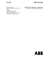
The Si5341/40 provides fault indicators which monitor loss of signal (LOS) of the inputs (IN0, IN1, IN2, XA/XB,
FB_IN) and loss of lock (LOL) for the PLL. This is shown in Figure 9.
Figure 9. LOS and LOL Fault Monitors
4.4.1. Status Indicators
The state of the status monitors are accessible by reading registers through the serial interface or with dedicated
pin (LOL). Each of the status indicator register bits has a corresponding sticky bit in a separate register location.
Once a status bit is asserted its corresponding sticky bit will remain asserted until cleared. Writing a logic zero to a
sticky register bit clears its state.
4.4.2. Interrupt pin (INTR)
An interrupt pin (INTR) indicates a change in state with any of the status registers. All status registers are maskable
to prevent assertion of the interrupt pin. The state of the INTR pin is reset by clearing the status registers.
Table 14. Manual Input Selection Using IN_SEL[1:0] Pins
IN_SEL[1:0]
Selected Input
Comment
0
0
IN0
Synchronous mode
0
1
IN1
1
0
IN2
1
1
XA/XB
Free-run mode (default)
PLL
LPF
PD
Mn
IN0
IN0
LOS0
÷P
0
IN1
IN1
÷P
1
FB_IN
FB_IN
IN2
IN2
÷P
2
LOL
Si5341/40
XB
XA
OSC
÷P
fb
Md
÷
LOSXAB
LOS1
LOS2
LOSFB
LO
L
LO
S0
LO
S1
LO
S2
L
O
SXA
B
IN
TR