


Circuit Operating Descriptions
13-15
Samsung Electronics
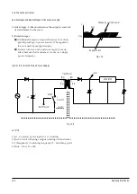
Fig. 13-17 Clock Control and Power Failure Detection
C624
C625
R657
IC608
7042
C688
14
16
15
85
86
1
2
3
61
BACKUP DET
AL5.8V
BUSY
D692
D620
(27) 4H’D Control
During trick play (Still, Slow, F-Advance), it is necessary to control pre-amp, Video circuit.
The Micom control pin 29 (C-ROTARY), pin 30 (HD-AMP) of the IC601 during PB period in Slow mode.
These port is applied to Video IC to operate the trick play.
(24) Timer/OTR Control
The timer can preset 6 programs in one year including daily and weekly programs.
Express recording lets the operator record up to 9 hours without programming the timer.
(25) Clock Display
The clock generator inside of the u-COM counts the oscillation signal of XT601 for the timer clock data.
(26) Power Failure Detection
u-COM goes to the power failure mode when the 61 port is lower than 4/5 of AD Vcc level.
Содержание DVD-V5450
Страница 23: ...Reference Information 14 12 Samsung Electronics Fig 14 14 Mecha Timing Chart Kaiser II ...
Страница 37: ...Reference Information 14 26 Samsung Electronics MEMO ...
Страница 49: ...Product Specification 2 12 Samsung Electronics MEMO ...
Страница 109: ...Operating Instructions 12 60 Samsung Electronics MEMO ...
Страница 158: ...Circuit Operating Descriptions 13 7 Samsung Electronics Fig 13 12 Block Diagram CASSET SWITCH START SEN ...
Страница 192: ...Circuit Operating Descriptions 13 41 Samsung Electronics 3 Block Diagram Fig 13 38 LA70100M Block Diagram ...
Страница 237: ...Troubleshooting 5 34 Samsung Electronics MEMO ...
Страница 247: ...Exploded View and Parts List 6 10 Samsung Electronics MEMO ...
Страница 261: ...7 14 Samsung Electronics Electrical Parts List This Document can not be used without Samsung s authorization MEMO ...
Страница 263: ...Block Diagram 8 2 MEMO Samsung Electronics ...
Страница 264: ...10 1 10 PCB Diagrams 10 1 VCR Main PCB 10 2 DVD Main PCB 10 3 Front PCB 10 2 10 4 10 6 Samsung Electronics ...
Страница 265: ...PCB Diagrams 10 2 Samsung Electronics 10 1 VCR Main PCB COMPONENT SIDE ...
Страница 266: ...PCB Diagrams 10 3 Samsung Electronics CONDUCTOR SIDE ...
Страница 267: ...PCB Diagrams 10 4 Samsung Electronics 10 2 DVD Main PCB COMPONENT SIDE ...
Страница 268: ...PCB Diagrams 10 5 Samsung Electronics CONDUCTOR SIDE ...
Страница 270: ...9 1 9 Wiring Diagram Samsung Electronics ...
Страница 271: ...Wiring Diagram 9 2 MEMO Samsung Electronics ...
Страница 273: ...Schematic Diagrams 11 2 This Document can not be used without Samsung s authorization Samsung Electronics 11 1 S M P S ...
Страница 276: ...Schematic Diagrams 11 5 This Document can not be used without Samsung s authorization Samsung Electronics 11 4 Logic ...
Страница 277: ...Schematic Diagrams 11 6 This Document can not be used without Samsung s authorization Samsung Electronics 11 5 A V ...
Страница 278: ...Schematic Diagrams 11 7 This Document can not be used without Samsung s authorization Samsung Electronics 11 6 Hi Fi ...
Страница 279: ...Schematic Diagrams 11 8 This Document can not be used without Samsung s authorization Samsung Electronics 11 7 A2 NICAM ...
Страница 282: ...Schematic Diagrams 11 11 This Document can not be used without Samsung s authorization Samsung Electronics 11 10 TM ...
Страница 283: ...Schematic Diagrams 11 12 This Document can not be used without Samsung s authorization Samsung Electronics 11 11 I O ...


