


4-8
Disassembly and Reassembly
Samsung Electronics
Œ
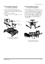
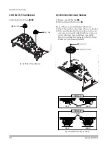
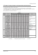
GEAR FL CAM
GEAR WORM WHEEL
POST
TIMING POINT
Fig. 4-15 Gear FL Cam, Gear Worm
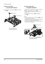
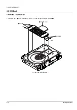
4-4-4 Slider FL Drive, Gear FL Cam Removal
1) Pull the Slider FL Drive
Œ
to the front direction.
2) Remove the Slider FL Drive
Œ
in the direction of
arrow. (Refer to Fig. 4-13)
3) Remove the Gear FL cam
´
.
Note
: When reinstalling be sure to reassemble Slider
FL drive
Œ
after you insert the Boss of Lever FL
ARM-R in Groove of Slider Fl drive
Œ
.
Assembly
: Align the Gear FL Cam
Œ
with the Gear
worm wheel Post as shown drawing.
(Refer to Timing point)
Œ
SLIDER FL DRIVE
´
GEAR FL CAM
Fig.4-14 Slider FL Drive Removal
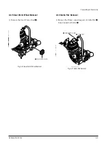
4-4-3 Lever FL Door Removal
1) Release the Hook
´
and Remove the Lever FL
Door
Œ
in the direction of arrow “A”.
Fig.4-13 Lever FL Door Removal
"B"
"C"
"A"
´
LEVER FL DOOR
Œ
SLIDER FL DRIVE
Содержание DVD-V5450
Страница 23: ...Reference Information 14 12 Samsung Electronics Fig 14 14 Mecha Timing Chart Kaiser II ...
Страница 37: ...Reference Information 14 26 Samsung Electronics MEMO ...
Страница 49: ...Product Specification 2 12 Samsung Electronics MEMO ...
Страница 109: ...Operating Instructions 12 60 Samsung Electronics MEMO ...
Страница 158: ...Circuit Operating Descriptions 13 7 Samsung Electronics Fig 13 12 Block Diagram CASSET SWITCH START SEN ...
Страница 192: ...Circuit Operating Descriptions 13 41 Samsung Electronics 3 Block Diagram Fig 13 38 LA70100M Block Diagram ...
Страница 237: ...Troubleshooting 5 34 Samsung Electronics MEMO ...
Страница 247: ...Exploded View and Parts List 6 10 Samsung Electronics MEMO ...
Страница 261: ...7 14 Samsung Electronics Electrical Parts List This Document can not be used without Samsung s authorization MEMO ...
Страница 263: ...Block Diagram 8 2 MEMO Samsung Electronics ...
Страница 264: ...10 1 10 PCB Diagrams 10 1 VCR Main PCB 10 2 DVD Main PCB 10 3 Front PCB 10 2 10 4 10 6 Samsung Electronics ...
Страница 265: ...PCB Diagrams 10 2 Samsung Electronics 10 1 VCR Main PCB COMPONENT SIDE ...
Страница 266: ...PCB Diagrams 10 3 Samsung Electronics CONDUCTOR SIDE ...
Страница 267: ...PCB Diagrams 10 4 Samsung Electronics 10 2 DVD Main PCB COMPONENT SIDE ...
Страница 268: ...PCB Diagrams 10 5 Samsung Electronics CONDUCTOR SIDE ...
Страница 270: ...9 1 9 Wiring Diagram Samsung Electronics ...
Страница 271: ...Wiring Diagram 9 2 MEMO Samsung Electronics ...
Страница 273: ...Schematic Diagrams 11 2 This Document can not be used without Samsung s authorization Samsung Electronics 11 1 S M P S ...
Страница 276: ...Schematic Diagrams 11 5 This Document can not be used without Samsung s authorization Samsung Electronics 11 4 Logic ...
Страница 277: ...Schematic Diagrams 11 6 This Document can not be used without Samsung s authorization Samsung Electronics 11 5 A V ...
Страница 278: ...Schematic Diagrams 11 7 This Document can not be used without Samsung s authorization Samsung Electronics 11 6 Hi Fi ...
Страница 279: ...Schematic Diagrams 11 8 This Document can not be used without Samsung s authorization Samsung Electronics 11 7 A2 NICAM ...
Страница 282: ...Schematic Diagrams 11 11 This Document can not be used without Samsung s authorization Samsung Electronics 11 10 TM ...
Страница 283: ...Schematic Diagrams 11 12 This Document can not be used without Samsung s authorization Samsung Electronics 11 11 I O ...


