


Circuit Operating Descriptions
13-3
Samsung Electronics
(2) Circuit description (FLY-Back PWM (Pulse Width Modulation control)
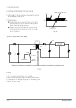
(a) AC Power Rectification/Smoothing Terminal
1) D1SS01, D1SS02, D1SS03, D1SS04 : Convert AC power to DC(Wave rectification).
2) C1SS10 : Smooth the voltage converted to DC.
3) L1SS01, L1SS02, C1SS01, C1SS02 : Noise removal at power input/output.
4) R1SS01 : Rush current limit resistance at the moment of power cord insertion.
- Without R1SS01, the bridge diode might be damaged as the rush current increases.
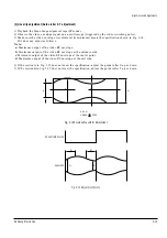
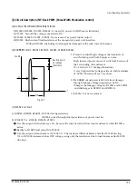
(b) SNUBBER Circuit : R1SD11, R1SD13, C1SD12, C1SD16, D1SS11
0
Vswitch
dt
Toff
t
Inverted power
by leakage
inductance
Fig. 13-7
1) Prevent residual high voltage at the terminals of
switch during switch off/Suppress noise.
High inverted power occurs at switch off, because of
the 1st winding of transformer :
(V= LI xdi/dt. LI : Leakage Induction)
A very high residual voltage exists on both terminals
of SCS11A because dt is a very short.
2) SNUBBER circuit protects SCS11A from damage
through leakage voltage suppression by RC,
(Charges the leakage voltage to D1SS11 and C1SD12
and discharges to R1SD11 and R1SD13).
3) C1SS16 : For noise removal
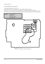
(c) IC1SS2 Vcc circuit
1) R1SR01, R1SR02, R1SR03 : IC1SS2 driving resistance
(IC1SS2 works through driving resistance at power cord in)
2) IC1SF01 Vcc : R1SS08, D1SF02, C1SF02
Œ
Use the output of transformer as Vcc, because the current starts to flow into transformer while IC1SS2 is
active.
´
Rectify to D1SF02 and smooth to C1SF02.
ˇ
Use the output of transformer as IC1SS2 Vcc : The loads are different before and after IC1SS2 driving.
(Vcc of IC1SS2 decreases below OFF voltage, using only the resistrance due to load increase after IC1SS2
driving.)
Содержание DVD-V5450
Страница 23: ...Reference Information 14 12 Samsung Electronics Fig 14 14 Mecha Timing Chart Kaiser II ...
Страница 37: ...Reference Information 14 26 Samsung Electronics MEMO ...
Страница 49: ...Product Specification 2 12 Samsung Electronics MEMO ...
Страница 109: ...Operating Instructions 12 60 Samsung Electronics MEMO ...
Страница 158: ...Circuit Operating Descriptions 13 7 Samsung Electronics Fig 13 12 Block Diagram CASSET SWITCH START SEN ...
Страница 192: ...Circuit Operating Descriptions 13 41 Samsung Electronics 3 Block Diagram Fig 13 38 LA70100M Block Diagram ...
Страница 237: ...Troubleshooting 5 34 Samsung Electronics MEMO ...
Страница 247: ...Exploded View and Parts List 6 10 Samsung Electronics MEMO ...
Страница 261: ...7 14 Samsung Electronics Electrical Parts List This Document can not be used without Samsung s authorization MEMO ...
Страница 263: ...Block Diagram 8 2 MEMO Samsung Electronics ...
Страница 264: ...10 1 10 PCB Diagrams 10 1 VCR Main PCB 10 2 DVD Main PCB 10 3 Front PCB 10 2 10 4 10 6 Samsung Electronics ...
Страница 265: ...PCB Diagrams 10 2 Samsung Electronics 10 1 VCR Main PCB COMPONENT SIDE ...
Страница 266: ...PCB Diagrams 10 3 Samsung Electronics CONDUCTOR SIDE ...
Страница 267: ...PCB Diagrams 10 4 Samsung Electronics 10 2 DVD Main PCB COMPONENT SIDE ...
Страница 268: ...PCB Diagrams 10 5 Samsung Electronics CONDUCTOR SIDE ...
Страница 270: ...9 1 9 Wiring Diagram Samsung Electronics ...
Страница 271: ...Wiring Diagram 9 2 MEMO Samsung Electronics ...
Страница 273: ...Schematic Diagrams 11 2 This Document can not be used without Samsung s authorization Samsung Electronics 11 1 S M P S ...
Страница 276: ...Schematic Diagrams 11 5 This Document can not be used without Samsung s authorization Samsung Electronics 11 4 Logic ...
Страница 277: ...Schematic Diagrams 11 6 This Document can not be used without Samsung s authorization Samsung Electronics 11 5 A V ...
Страница 278: ...Schematic Diagrams 11 7 This Document can not be used without Samsung s authorization Samsung Electronics 11 6 Hi Fi ...
Страница 279: ...Schematic Diagrams 11 8 This Document can not be used without Samsung s authorization Samsung Electronics 11 7 A2 NICAM ...
Страница 282: ...Schematic Diagrams 11 11 This Document can not be used without Samsung s authorization Samsung Electronics 11 10 TM ...
Страница 283: ...Schematic Diagrams 11 12 This Document can not be used without Samsung s authorization Samsung Electronics 11 11 I O ...


