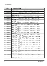
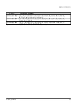


Circuit Operating Descriptions
13-2
Samsung Electronics
◆
Advantages and disadvantages of linear power supply
1) Advantages : Little noise because the output waveform
of transformer is sine wave.
2) Disadvantages :
Œ
Additional margin is required because Vs is chan-
ged (depending on power source). (The regulator
loss is caused by margin design).
´
Greater core size and condensor capacity are ne-
eded, because the transformer works on a single
power frequency.
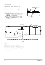
(b) S.M.P.S. (Switch Mode Power Supply)
v
Vreg
Vout
0
t
Change by common power
Regulator loss
Fig. 13-5
◆
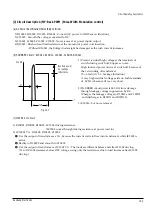
Terms
1) 1st : Common power input to 1st winding.
2) 2nd : Circuit followings output winding of transformer.
3) f (Frequency) : Switching frequency (T : Switching cycle)
4) Duty : (Ton/T) x 100
Transformer
Vout
(Np)
(Vp)
Switch
Vs switch
I switch
Vin
ON/OFF Control
+
–
+
–
+
+
+
–
(Vs)
(Ns)
REGULATOR
Fig. 13-6
Содержание DVD-V5450
Страница 23: ...Reference Information 14 12 Samsung Electronics Fig 14 14 Mecha Timing Chart Kaiser II ...
Страница 37: ...Reference Information 14 26 Samsung Electronics MEMO ...
Страница 49: ...Product Specification 2 12 Samsung Electronics MEMO ...
Страница 109: ...Operating Instructions 12 60 Samsung Electronics MEMO ...
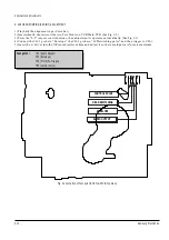
Страница 158: ...Circuit Operating Descriptions 13 7 Samsung Electronics Fig 13 12 Block Diagram CASSET SWITCH START SEN ...
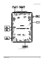
Страница 192: ...Circuit Operating Descriptions 13 41 Samsung Electronics 3 Block Diagram Fig 13 38 LA70100M Block Diagram ...
Страница 237: ...Troubleshooting 5 34 Samsung Electronics MEMO ...
Страница 247: ...Exploded View and Parts List 6 10 Samsung Electronics MEMO ...
Страница 261: ...7 14 Samsung Electronics Electrical Parts List This Document can not be used without Samsung s authorization MEMO ...
Страница 263: ...Block Diagram 8 2 MEMO Samsung Electronics ...
Страница 264: ...10 1 10 PCB Diagrams 10 1 VCR Main PCB 10 2 DVD Main PCB 10 3 Front PCB 10 2 10 4 10 6 Samsung Electronics ...
Страница 265: ...PCB Diagrams 10 2 Samsung Electronics 10 1 VCR Main PCB COMPONENT SIDE ...
Страница 266: ...PCB Diagrams 10 3 Samsung Electronics CONDUCTOR SIDE ...
Страница 267: ...PCB Diagrams 10 4 Samsung Electronics 10 2 DVD Main PCB COMPONENT SIDE ...
Страница 268: ...PCB Diagrams 10 5 Samsung Electronics CONDUCTOR SIDE ...
Страница 270: ...9 1 9 Wiring Diagram Samsung Electronics ...
Страница 271: ...Wiring Diagram 9 2 MEMO Samsung Electronics ...
Страница 273: ...Schematic Diagrams 11 2 This Document can not be used without Samsung s authorization Samsung Electronics 11 1 S M P S ...
Страница 276: ...Schematic Diagrams 11 5 This Document can not be used without Samsung s authorization Samsung Electronics 11 4 Logic ...
Страница 277: ...Schematic Diagrams 11 6 This Document can not be used without Samsung s authorization Samsung Electronics 11 5 A V ...
Страница 278: ...Schematic Diagrams 11 7 This Document can not be used without Samsung s authorization Samsung Electronics 11 6 Hi Fi ...
Страница 279: ...Schematic Diagrams 11 8 This Document can not be used without Samsung s authorization Samsung Electronics 11 7 A2 NICAM ...
Страница 282: ...Schematic Diagrams 11 11 This Document can not be used without Samsung s authorization Samsung Electronics 11 10 TM ...
Страница 283: ...Schematic Diagrams 11 12 This Document can not be used without Samsung s authorization Samsung Electronics 11 11 I O ...


