


Circuit Operating Descriptions
13-4
Samsung Electronics
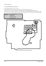
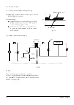
1) F/B terminal of IC1SF01 determines output duty cycle.
2) C-E(Collector-Emitter) of IC1SF01 and F/B potential of IC1SF01 are same.
◆
Operation descriptions
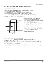
1) Internal OP-Amp ‘+’ base potential of IC1S03 is 2.5V and external “-” input potential is connected with
R1SS35 and R1SS34 to maintain Vout of 5.8V. (Vout = (((R1SS34)xR1SS35 ) / R1SS35) x 2.5V)
2) If load of 5.8 V terminal increases(or AC input voltage decreases) and Vout decreases below 5.8V, then :
IC1S03 “P” potential down below 2.5V --> IC1S03 A-K of base current down --> IC1S03 of A-K current down
--> IC1S03 Diode current down --> IC1S03 C-E current down --> IC1S03 C-E voltage up --> IC1SS2 F/B voltage
up --> Out Duty up --> Transformer 1st current up --> Transformer 1st power up --> Vout up --> Maintain Vout
5.8V
3) If load of 5.8 V terminal decreases(or AC input voltage rises) and Vout rises above 5.8V, then :
Reverse sequence of the above description --> Duty down --> Vout down --> Maintain 5.8V (i.e., the feedback
to maintains 5.8V).
Œ
R1SS33, R1SS31 : Reduce 5.8V overshoot
´
R1SS32, C1SS27 : Prevent IC1S03 oscillation(for phase correction)
(d) Feedback Control Circuit
IC1SS2
OCP
DRAIN
F/B
IC1S02
C
E
1st GND
A
K
IC1S03
A
2.5V
K
R
R1SS32
C1SS27
2nd GND
R1SS35
R1SS33
R1SS31
R1SS34
C1SS16
5.8V
L1SS05
D1SS13
C1SS35
Trans
GND
$
@
*
%
#
VCC
&
Fig. 13-8
Содержание DVD-V5450
Страница 23: ...Reference Information 14 12 Samsung Electronics Fig 14 14 Mecha Timing Chart Kaiser II ...
Страница 37: ...Reference Information 14 26 Samsung Electronics MEMO ...
Страница 49: ...Product Specification 2 12 Samsung Electronics MEMO ...
Страница 109: ...Operating Instructions 12 60 Samsung Electronics MEMO ...
Страница 158: ...Circuit Operating Descriptions 13 7 Samsung Electronics Fig 13 12 Block Diagram CASSET SWITCH START SEN ...
Страница 192: ...Circuit Operating Descriptions 13 41 Samsung Electronics 3 Block Diagram Fig 13 38 LA70100M Block Diagram ...
Страница 237: ...Troubleshooting 5 34 Samsung Electronics MEMO ...
Страница 247: ...Exploded View and Parts List 6 10 Samsung Electronics MEMO ...
Страница 261: ...7 14 Samsung Electronics Electrical Parts List This Document can not be used without Samsung s authorization MEMO ...
Страница 263: ...Block Diagram 8 2 MEMO Samsung Electronics ...
Страница 264: ...10 1 10 PCB Diagrams 10 1 VCR Main PCB 10 2 DVD Main PCB 10 3 Front PCB 10 2 10 4 10 6 Samsung Electronics ...
Страница 265: ...PCB Diagrams 10 2 Samsung Electronics 10 1 VCR Main PCB COMPONENT SIDE ...
Страница 266: ...PCB Diagrams 10 3 Samsung Electronics CONDUCTOR SIDE ...
Страница 267: ...PCB Diagrams 10 4 Samsung Electronics 10 2 DVD Main PCB COMPONENT SIDE ...
Страница 268: ...PCB Diagrams 10 5 Samsung Electronics CONDUCTOR SIDE ...
Страница 270: ...9 1 9 Wiring Diagram Samsung Electronics ...
Страница 271: ...Wiring Diagram 9 2 MEMO Samsung Electronics ...
Страница 273: ...Schematic Diagrams 11 2 This Document can not be used without Samsung s authorization Samsung Electronics 11 1 S M P S ...
Страница 276: ...Schematic Diagrams 11 5 This Document can not be used without Samsung s authorization Samsung Electronics 11 4 Logic ...
Страница 277: ...Schematic Diagrams 11 6 This Document can not be used without Samsung s authorization Samsung Electronics 11 5 A V ...
Страница 278: ...Schematic Diagrams 11 7 This Document can not be used without Samsung s authorization Samsung Electronics 11 6 Hi Fi ...
Страница 279: ...Schematic Diagrams 11 8 This Document can not be used without Samsung s authorization Samsung Electronics 11 7 A2 NICAM ...
Страница 282: ...Schematic Diagrams 11 11 This Document can not be used without Samsung s authorization Samsung Electronics 11 10 TM ...
Страница 283: ...Schematic Diagrams 11 12 This Document can not be used without Samsung s authorization Samsung Electronics 11 11 I O ...