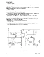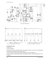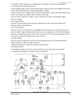
The MOSFET cuts OFF when the current increases and the voltage at Pin 1 of the IC exceeds the set point.
The IC acts as a QRC (Quasi-Resonant Control).
Constant voltage regulation occurs through the switching ON/OFF of the photo-coupler PC8431 according to the
output voltage that has been resistor divided (R8433, R8434, and R8435).
When the output voltage increases, the photo-coupler (PC8431) turns ON in order to increase the voltage at Pin 5
of the IC which narrows down the ON width for limited output voltage.
When the output voltage drops, it reverses in order to widen the ON width for increased output voltage.
[Protection Features]
-Over Voltage Protection
The Latch circuit is activated in order to stop the circuit when the Vcc terminal voltage exceeds the OVP
activating voltage Vcc(OVP)=28V(TYP).
-Over Current Protection
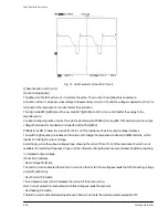
A pulse by pulse over-current protection circuit detects the peak value of the drain current of the FET per every
pulse. The detection resistors R8301& RX8301 convert the current to voltage and Pin 2 of the STR-F6267 detects it.
When this value exceeds the set point, FET cuts OFF to cut out the current in order to be released again to ON by
the next cycle. Repeating OFF and ON results in the current limit.
-Overload Protection
The UVLO (Under Voltage Lockout) occurs during the overload status (the drain current is limited by OCP
behavior) caused by a malfunction of the loading side.
This feature protects the IC in case of an overload to the secondary side.
-Overheating Protection
For overheating protection, the latch circuit is activated when the temperature of the chip exceeds 140°….
The actual temperature detection is done by the control circuit element.
Fig. 9. QRC Circuit (Primary)
Samsung Electronics 6-
15
Circuit Operation Description
Содержание D61B
Страница 10: ...3 2 Samsung Electronics MEMO ...
Страница 20: ...4 10 Samsung Electronics 4 11 1Sub field Process Address 1 4 12 1Sub field Process Address 2 Introduction PDP ...
Страница 21: ...Introduction PDP Samsung Electronics 4 11 4 13 1Sub field Process Address 3 4 14 1Sub field Process Address 4 ...
Страница 22: ...Introduction PDP 4 12 Samsung Electronics 4 15 1Sub field Process Address 5 4 16 1Sub field Process Address 6 ...
Страница 23: ...Introduction PDP Samsung Electronics 4 13 4 17 1Sub field Process Address 7 4 18 1Sub field Process Address 8 ...
Страница 24: ...Introduction PDP 4 14 Samsung Electronics 4 20 1Sub field Process Sustain 4 19 1Sub field Process Address 9 ...
Страница 30: ...4 20 Samsung Electronics MEMO ...
Страница 38: ...Alignment and Adjustments 2 8 Samsung Electronics MEMO ...
Страница 61: ...Fig 18 Chopper Circuit 6 22 Samsung Electronics Circuit Operation Description ...
Страница 85: ...8 8 Samsung Electronics MEMO ...
Страница 99: ...9 14 Samsung Electronics MEMO ...
Страница 105: ...Schematic Diagrams 10 6 Samsung Electronics 10 6 SMPS 1 This Document can not be used without Samsung s authorization ...
Страница 106: ...Samsung Electronics Schematic Diagrams 10 7 10 7 SMPS 2 ...
Страница 107: ...Schematic Diagrams 10 8 Samsung Electronics 10 8 SMPS 3 ...
Страница 108: ...Samsung Electronics Schematic Diagrams 10 9 10 9 SMPS 4 ...


